ВУЗ: Казахская Национальная Академия Искусств им. Т. Жургенова
Категория: Книга
Дисциплина: Не указана
Добавлен: 03.02.2019
Просмотров: 21623
Скачиваний: 19

12-18 Broadcast Receiver Systems
products are negligibly affected by those filters. For this reason, odd-order products are generally
much more troublesome than even-order products and are tested for more frequently. The sec-
ond- and third-order products are generally the strongest and are the ones most frequently tested.
A two-signal generator test set is required for testing, depending on the details of the specified
test.
For IM measurements, the controls of the receiver under test are set to the specified band-
widths, operating frequency, and other settings as appropriate, and the gain control is set on man-
ual (or AGC disabled). One signal generator is set on the operating frequency, modulated and
adjusted to provide a specified S/N (that for sensitivity, for example). The modulation is dis-
abled, and the output level of this signal is measured. This must be done using the IF output, the
SSB output with the signal generator offset by a convenient audio frequency, or with the BFO on
and offset. Alternatively, the dc level at the AM demodulator can be measured, if accessible. The
signal generator is then turned off. It may be left off during the remainder of the test or retuned
and used to produce one of the interfering signals.
For second-order IM testing, two signal generators are now set to two frequencies differing
from each other by the operating frequency. These frequencies can be equally above and below
the carrier frequency at the start, and shifted on successive tests to assure that the preselection
filters do not have any weak regions. The signal with the frequency nearest to the operating fre-
quency must be separated far enough to assure adequate channel filter attenuation of the signal
(several channels). For third-order IM testing, the frequencies are selected in accordance with the
formula given previously so that the one further from the operating frequency is twice as far as
the one nearer to the operating frequency. For example, the nearer interferer might be three chan-
nels from the desired frequency and the further one, six channels in the same direction.
In either case, the voltage levels of the two interfering signal generators are set equal and are
gradually increased until an output equal to the original channel output is measured in the chan-
nel. One of several performance requirements may be specified. If the original level is the sensi-
tivity level, the ratio of the interfering generator level to the sensitivity level may have a specified
minimum. Alternatively, for any original level, an interfering generator level may be specified
that must not produce an output greater than the original level. Finally, an intercept point (IP)
may be specified.
The IP for the nth order of intermodulation occurs because the product is a result of the inter-
fering signal voltages being raised to the nth power. With equal voltages, as in the test, the result-
ant output level of the product increases as
(12.1.7)
where c
n
is a proportionality constant and V is the common input level of the two signals.
Because the output from a single signal input V at the operating frequency is G
vV
, there is a theo-
retical level at which the two outputs would be equal. This value V
IPn
is the nth IP, measured at
the input. It is usually specified in dBm. In practice the IPs are not reached because as the ampli-
fiers approach saturation, the voltage at each measured frequency becomes a combination of
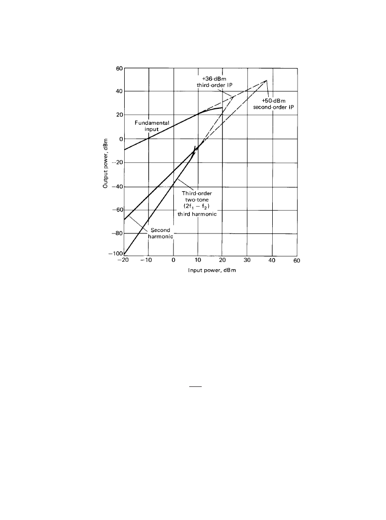
components from various orders of n. Figure 12.1.5 indicates the input-output power relation-
ships in second- and third-order IPs.
In Equation 12.1.7 we note that at the IP
V
c V
dn
n
n
=
Downloaded from Digital Engineering Library @ McGraw-Hill (www.digitalengineeringlibrary.com)
Copyright © 2004 The McGraw-Hill Companies. All rights reserved.
Any use is subject to the Terms of Use as given at the website.
Receiver Characteristics

Receiver Characteristics 12-19
(12.1.8)
This leads to
(12.1.9)
The ratio of signal to distortion becomes
. In decibels it becomes
V
c
V
dn
n
IPn
n
=
(
) and (
)
(
)
V
G
V
IPn
out
v
IPn
in
=
c
G
V
n
v
IPn
n
=
(
)
–
1
and V
G V
V
V
dn
v
IPn
n
=
1 –
V
IPn
(
) V
n
1
–
⁄
Figure 12.1.5
Input/output power relationships for second- and third-order intercept points.
Downloaded from Digital Engineering Library @ McGraw-Hill (www.digitalengineeringlibrary.com)
Copyright © 2004 The McGraw-Hill Companies. All rights reserved.
Any use is subject to the Terms of Use as given at the website.
Receiver Characteristics

12-20 Broadcast Receiver Systems
(12.1.10)
If the intercept level is expressed in dBm rather than voltage, then the output power represented
by V must be similarly expressed.
The IM products we have been discussing originate in the active devices of the receiver, so
that the various voltages or power levels are naturally measured at the device output. The IP is
thus naturally referred to the device output and is so specified in most data sheets. In the forego-
ing discussion, we have referred the IP to the voltage level at the device input. If the input power
is required, we subtract from the output intercept level in decibels, the amplifier power gain or
loss. The relationship between input and output voltage at the IP is given in Equation 12.1.8. Ref-
erence of the IP to the device input is somewhat unnatural but is technically useful because the
receiver system designer must deal with the IP generation in all stages and needs to know at what
antenna signal level the receiver will produce the maximum tolerable IM products.
Consider the input power (in each signal) that produces an output IM product equal to the
MDS. The ratio of this power to the MDS may be called the third-order IM dynamic range. It
also is sometimes referred to as the two-tone dynamic range. Expressing Equation 12.1.10 in
terms of input power and input IP measured in dBm, we have
(12.1.11)
When we substitute MDS for the distortion and MDS + DR for P
(in)
we obtain
(12.1.12)
When n is 3, we find the relationship
(12.1.13)
A dynamic range could presumably be defined for other orders of IM, but it is not common to do
so. From the three different definitions of dynamic range described in this section, it should be
clear why it is important to be careful when comparing receiver specifications for this character-
istic.
R
V
V
n
V
V
dn
dn
IPn
=
=
20
1 20
20
log
( – ) [
log
–
log
]
R
n
IP
P
dn
n in
in
=( – ) [
–
]
(
)
(
)
1
DR
n
IP
MDS
DR
n in
=( – ) [
–
–
]
(
)
1
,
nDR
n
IP
MDS
n in
=( – ) [
–
]
(
)
1
DR
IP
MDS
in
=
2
3
3
[
–
]
(
)
Downloaded from Digital Engineering Library @ McGraw-Hill (www.digitalengineeringlibrary.com)
Copyright © 2004 The McGraw-Hill Companies. All rights reserved.
Any use is subject to the Terms of Use as given at the website.
Receiver Characteristics

Receiver Characteristics 12-21
12.1.4d
Error Vector Magnitude
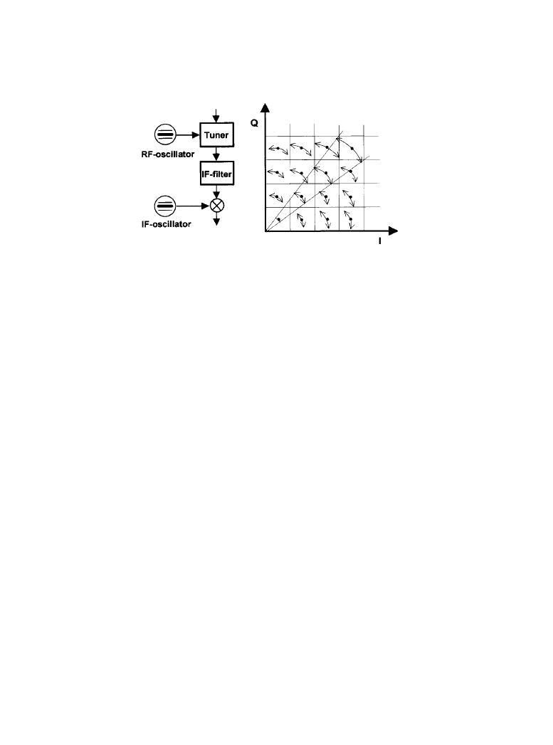
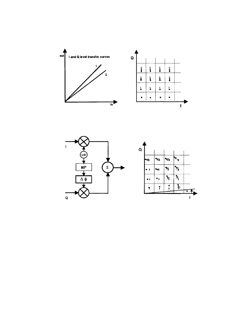
As shown in Figure 12.1.6, particular sources of amplitude and/or phase error can shift the val-
ues of digital emission data states toward decision boundaries, resulting in increased BER
because of intersymbol interference. Figures 12.1.7, 12.1.8, and 12.1.9 show three additional
sources of such errors.
A figure of merit known as error vector magnitude (EVM) has been developed as sensitive
indicator of the presence and severity of such errors. The error vector magnitude of an emission
is the magnitude of the phasor difference as a function of time between an ideal reference signal
and the measured transmitted signal after its timing, amplitude, frequency, phase, and dc offset
have been modified by circuitry and/or propagation. Figure 12.1.10 illustrates the EVM concept.
12.1.5 Gain Control
Receivers must often be capable of handling a signal range of 100 dB or more. Most amplifiers
remain linear over only a much smaller range. The later amplifiers in a receiver, which must pro-
vide the demodulator with about 1 V on weak signals, would need the capability to handle thou-
sands of volts for strong signals without some form of gain control. Consequently, receivers
customarily provide means for changing the gain of the RF or IF amplifiers, or both.
For applications where the received signal is expected to remain always within narrow limits,
some form of manually selectable control can be used, which may be set on installation and sel-
dom adjusted. There are few such applications. Most receivers, however, even when an operator
is available, must receive signals that vary by tens of decibels over periods of fractions of sec-
Figure 12.1.6
Ph
ase noise is critical to digitally modulated communication systems because
of the modulation errors it can introduce.
Inter-symbol interference (ISI), accompanied by a
rise in BER, results when state values become so badly error-blurred that they fall into the
regions of adjacent states. This drawing depicts only the results of phase errors introduced
by
phase noise; in actual systems, thermal noise, AM-to-PM conversion, differential group delay,
propagation, and other factors may also contribute to the spreading of state amplitude and
phase values. (
Courtesy of Rohde & Schwarz.)
Downloaded from Digital Engineering Library @ McGraw-Hill (www.digitalengineeringlibrary.com)
Copyright © 2004 The McGraw-Hill Companies. All rights reserved.
Any use is subject to the Terms of Use as given at the website.
Receiver Characteristics

12-22 Broadcast Receiver Systems
onds to minutes. The level also changes when the frequency is reset to receive other signals that
may vary over similar ranges but with substantially different average levels. Consequently, an
AGC is very desirable.
Some angle modulation receivers provide gain control by using amplifiers that limit on strong
signals. Because the information is in the angle of the carrier, the resulting amplitude distortion
is of little consequence. Receivers that must preserve AM or maintain very low angle modulation
distortion use amplifiers that can be varied in gain by an external control voltage. In some cases,
this has been accomplished by varying the operating points of the amplifying devices, but most
modern systems separate solid-state circuits or switched passive elements to obtain variable
attenuation between amplifier stages with minimum distortion. For manual control, provision
can be made to let an operator set the control voltage for these variable attenuators. For automatic
control, the output level from the IF amplifiers or the demodulator is monitored by the AGC cir-
Figure 12.1.7
Effect of gain imbalance between
I and Q channels on data signal phase con-stella-
tion. (
Courtesy of Rohde & Schwarz.)
Figure 12.1.8
Effect of quadrature offset on data signal phase constellation. (
Courtesy of Rohde &
Schwarz.)
Downloaded from Digital Engineering Library @ McGraw-Hill (www.digitalengineeringlibrary.com)
Copyright © 2004 The McGraw-Hill Companies. All rights reserved.
Any use is subject to the Terms of Use as given at the website.
Receiver Characteristics