ВУЗ: Казахская Национальная Академия Искусств им. Т. Жургенова
Категория: Книга
Дисциплина: Не указана
Добавлен: 03.02.2019
Просмотров: 21648
Скачиваний: 19

4-50 Microphone Devices and Systems
A portion of the output voltage may also be fed back to the input, which is the base or gate
terminal. This resistor R
f
will lower the input impedance of the single amplifier stage, reduce
current amplification, reduce output impedance of the stage, and act as a supply voltage source
for the base or gate. This method is used when the source of input signals and internal resistance
R
s
is coupled with a capacitor to the base or gate and a group of devices with a spread of current
gains, transconductances, or pinch-off voltages must operate with similar amplification in the
same circuit. If the feedback element is also a capacitor C
f
, high-frequency current amplification
of the stage will be reduced by approximately 3 dB when the impedance of the capacitor is equal
to the feedback resistor R
f
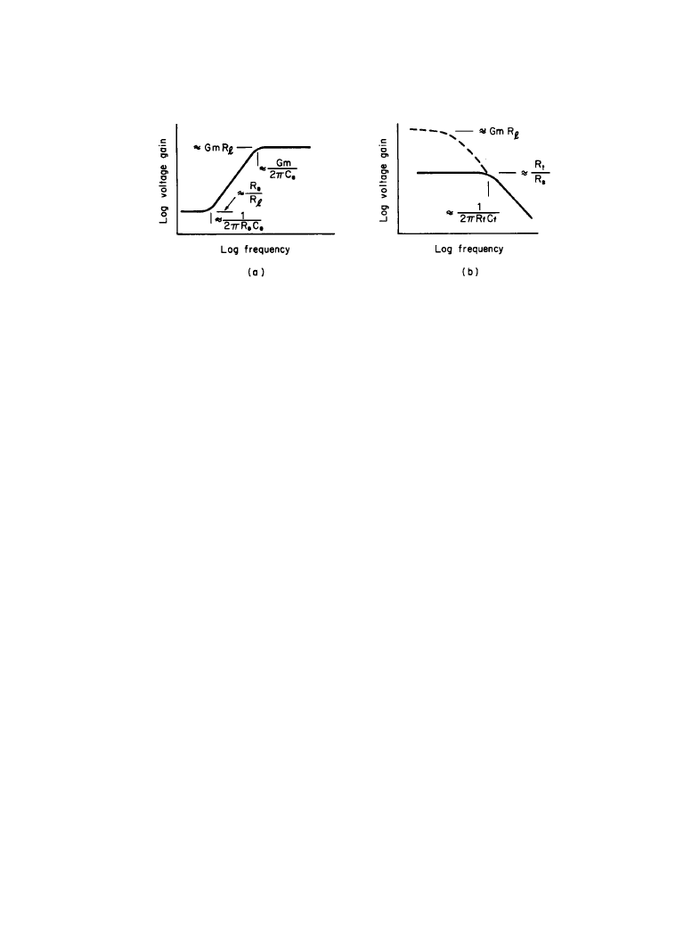
and voltage gain of the stage is high (Figure 4.3.2b). At still higher
frequencies amplification will decrease at the rate of 6 dB per octave of frequency. It should be
noted at this point that the base-collector or gate-drain capacitance of the device has the same
effect of limiting high-frequency amplification of the stage, but this capacitor becomes larger as
collector-base or drain-gate voltage decreases.
Feedback of the output voltage through an impedance lowers the input impedance of an
amplifier stage. Voltage amplification of the stage will be affected only as this lowered input
impedance loads the source of input voltage. If the source of input voltage has a finite source
impedance and the amplifier stage has very high voltage amplification and reversed phase, the
effective amplification for this stage will approach the ratio of feedback impedance to source
impedance and also have reversed phase.
Common-Base or Common-Gate Connection
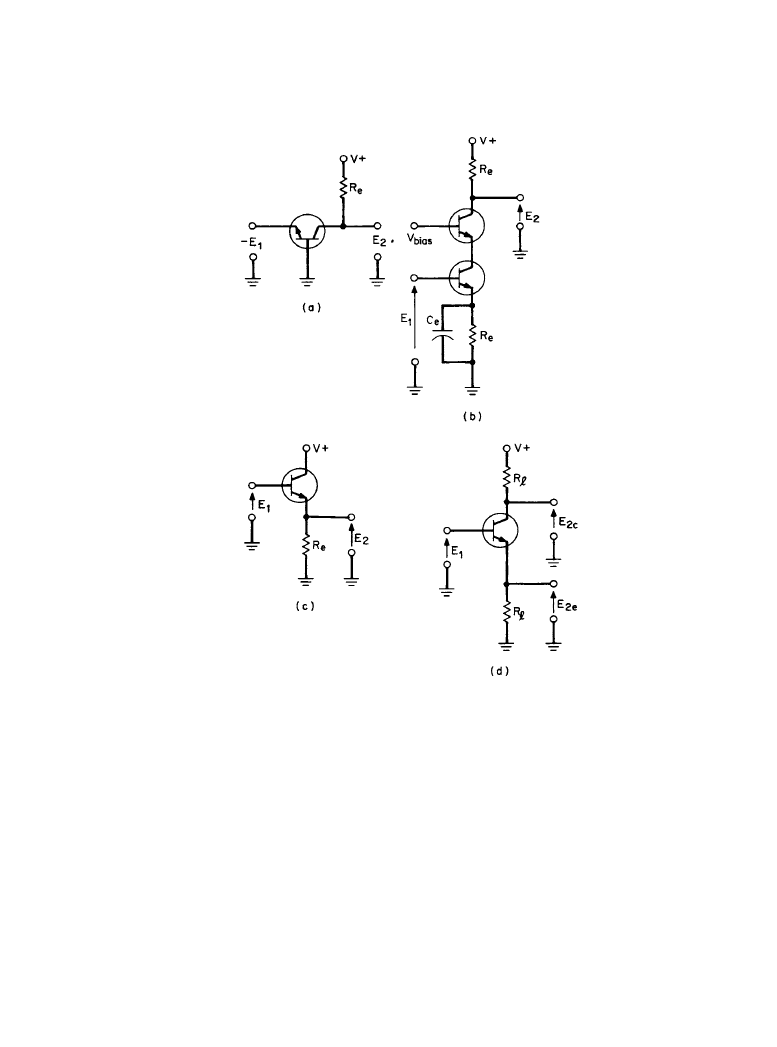
For this configuration (Figure 4.3.3a), voltage amplification is the same as in the common-emit-
ter or common-source connection, but input impedance is approximately the inverse of the
transconductance of the device. As a benefit, high-frequency amplification will be less affected
because of the relatively lower emitter-collector or source-drain capacitance and the relatively
low input impedance. This is the reason why the cascade connection (Figure 4.3.3b) of a com-
mon-emitter amplifier stage driving a common-base amplifier stage exhibits nearly the dc ampli-
fication of a common-emitter stage with the wide bandwidth of a common-base stage. The other
advantage of a common-base or common-gate amplifier stage is stable amplification at very
high frequencies (VHF) and ease of matching to transmission-line impedances, usually 50 to
75
Ω.
Figure 4.3.2
Feedback amplifier voltage gains: (
a) current feedback, (b) voltage feedback.
Downloaded from Digital Engineering Library @ McGraw-Hill (www.digitalengineeringlibrary.com)
Copyright © 2004 The McGraw-Hill Companies. All rights reserved.
Any use is subject to the Terms of Use as given at the website.
Low Power Amplifiers

Low Power Amplifiers 4-51
Common-Collector or Common-Drain Connection of a Transistor or FET
For this case, voltage gain is slightly below 1.000, but the input impedance of a transistor so con-
nected will be equal to the value of the load impedance multiplied by the current gain of the
device plus the inverse of the transconductance of the device (Figure 4.3.3c). Similarly, the out-
put impedance of the stage will be the impedance of the source of signals divided by the current
gain of the transistor plus the inverse of the transconductance of the device.
When identical resistors are connected between the collector or drain and the supply voltage
and the emitter or source and ground, an increase in base or gate voltage will result in an increase
of emitter or source voltage that is nearly equal to the decrease in collector or drain voltage. This
Figure 4.3.3
Transistor amplifier circuits: (
a) common-base NPN, (b) cascade NPN, (c) common-
collector NPN emitter follower, (
d) split-load phase inverter.
Downloaded from Digital Engineering Library @ McGraw-Hill (www.digitalengineeringlibrary.com)
Copyright © 2004 The McGraw-Hill Companies. All rights reserved.
Any use is subject to the Terms of Use as given at the website.
Low Power Amplifiers

4-52 Microphone Devices and Systems
type of connection is known as the split-load phase inverter, useful for driving push-pull amplifi-
ers, although the output impedances at the two output terminals are unequal (Figure 4.3.3d).
The current gain of a transistor decreases at high frequencies as the emitter-base capacitance
shunts a portion of the transconductance, thereby reducing current gain until it reaches a value of
1 at the transition frequency of the transistor (Figure 4.3.4). From this it can be seen that the out-
put impedance of an emitter-follower or common-collector stage will increase with frequency,
having the effect of an inductive source impedance when the input source to the stage is resistive.
If the source impedance is inductive, as it might be with cascaded emitter followers, the output
impedance of such a combination can be a negative value at certain high frequencies and be a
possible cause of amplifier oscillation. Similar considerations also apply to common-drain FET
stages.
Bias and Large Signals
When large signals have to be handled by a single-stage amplifier, distortion of the signals intro-
duced by the amplifier must be considered. Although feedback can reduce distortion, it is neces-
sary to ensure that each stage of amplification operates in a region where normal signals will not
cause the amplifier stage to operate with nearly zero voltage drop across the device or to operate
the device with nearly zero current during a portion of the cycle of the signal. Although the
amplifier is described primarily with respect to a single-device amplifier stage, the same holds
true for any amplifier stage with multiple devices, except that here at least one device must be
able to control current flow in the load without being saturated (nearly zero voltage drop) or cut
off (nearly zero current):
If the single-device amplifier load consists of the collector or drain load resistor only, the best
operating point should be chosen so that in the absence of a signal, one-half of the supply voltage
appears as a quiescent voltage across the load resistor R
1
. If an additional resistive load R
1
is con-
nected to the output through a coupling capacitor C
c
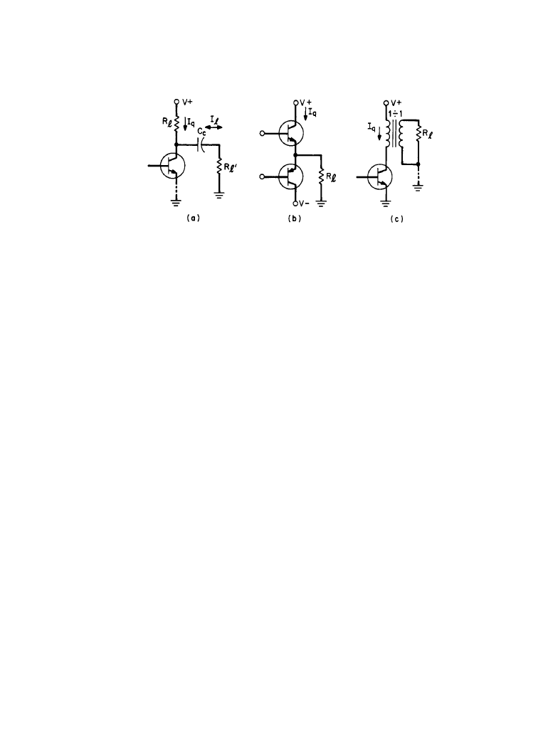
(Figure 4.3.5a), the maximum peak load
current 1
1
in one direction is equal to the difference between quiescent current I
q
of the stage and
the current that would flow if the collector resistor and the external load resistor were connected
in series across the supply voltage. In the other direction maximum load current is limited by the
quiescent voltage across the device divided by the load resistance. The quiescent current flows in
the absence of an alternating signal and is caused by bias voltage or current only. For signals with
an equal probability of positive and negative peak excursions, such as audio-frequency wave-
forms, it is advisable to have the two peak currents equal. This can be accomplished by increas-
ing the quiescent current as the external load resistance decreases.
When several devices contribute current into an external load resistor (Figure 4.3.5b), one
useful strategy is to set bias currents so that the sum of all transconductances remains as constant
Figure 4.3.4
Amplitude-frequency response of a com-
mon-emitter or common-source amplifier.
Downloaded from Digital Engineering Library @ McGraw-Hill (www.digitalengineeringlibrary.com)
Copyright © 2004 The McGraw-Hill Companies. All rights reserved.
Any use is subject to the Terms of Use as given at the website.
Low Power Amplifiers

Low Power Amplifiers 4-53
as practical, which means a design for minimum distortion. This operating point for one device
is near one-fourth of the peak device current for push-pull FET stages and at a lesser value for
bipolar push-pull amplifiers.
When the load resistance is coupled to the single-device amplifier stage with a transformer
(Figure 4.3.5c), the optimum bias current should be nearly equal to the peak current that would
flow through the load impedance at the primary of the transformer with a voltage drop equal to
the supply voltage.
4.3.2c
Multistage Amplifiers
All practical audio, video, and radio-frequency amplifiers are multistage amplifiers in which
cascaded single-stage amplifiers are connected together: Overall feedback then is used to stabi-
lize amplification and quiescent operating points [5].
DC-Coupled Multistage Amplifiers
Commonly, amplifier stages enclosed in an overall feedback loop are direct-coupled so that the
quiescent operating point is determined primarily by the bias of the first stage.
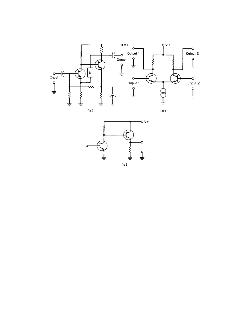
Two cascaded common-emitter amplifier stages can form a gain block useful as a low-cost
preamplifier (Figure 4.3.6a). Here, the collector of the first stage is connected to the base of the
second stage and to a resistor that supplies collector current to the first stage and base current to
the second stage from the supply voltage. Both stages have an emitter resistor connected to the
common ground, with the second resistor bypassed with a large capacitor. Base current to the
first stage is supplied from the emitter of the second stage through a pair of voltage-divider resis-
tors connected to ground, with audio input signals fed to the base of the first stage through a cou-
pling capacitor. The audio-signal output is taken from the collector of the second stage through a
coupling capacitor. The second collector receives its operating current through a resistor and
supplies feedback current through a resistor-capacitor network to the emitter of the first stage.
When using two NPN transistors and a single positive supply voltage, a low-cost preamplifier
with the appropriate feedback network is constructed. The maximum no-feedback voltage ampli-
Figure 4.3.5
Output load-coupling circuits: (
a) ac-coupled, (b) series-dc parallel-ac push-pull half
bridge, (
c) single-ended, transformer-coupled.
Downloaded from Digital Engineering Library @ McGraw-Hill (www.digitalengineeringlibrary.com)
Copyright © 2004 The McGraw-Hill Companies. All rights reserved.
Any use is subject to the Terms of Use as given at the website.
Low Power Amplifiers

4-54 Microphone Devices and Systems
fication is approximately equal to the transconductance of the first stage multiplied by the cur-
rent gain of the second stage and the load resistor value of the second stage.
When two transistors or FETs have their emitters or sources connected together and that junc-
tion is supplied with a constant current and output voltages are obtained from identical-value
resistors connected between the supply voltage and the two collectors or drains, the long-tailed-
pair or emitter-coupled or source-coupled phase-inverter stage is described (Figure 4.3.6b). Here
the emitter or source of one device acts as the emitter or source resistor for the other device, and
an alternating signal impressed on one input will be amplified with a phase reversal in the same
stage while this reversal is not experienced at the other output. This stage, then, is capable of tak-
ing one single-ended signal and transforming it into a push-pull signal. The signal applied to the
other input now will arrive at the first output without a phase reversal. Thus, the emitter- or
source-coupled amplifier is able to amplify the difference between two signals, where one may
be an input signal and the other a feedback signal. Its voltage amplification is the same as the
normal grounded emitter or grounded source stage, except that the output voltage should now be
measured between the two outputs, with the voltage from either output to ground being one-half
of that value. This type of input stage is the almost universal input stage of operational amplifi-
ers.
Figure 4.3.6
Multistage dc-coupled circuits: (
a) cascaded two-transistor amplifier, (b) emitter-cou-
pled phase inverter, (
c) cascade NPN and PNP transistors.
Downloaded from Digital Engineering Library @ McGraw-Hill (www.digitalengineeringlibrary.com)
Copyright © 2004 The McGraw-Hill Companies. All rights reserved.
Any use is subject to the Terms of Use as given at the website.
Low Power Amplifiers