ВУЗ: Казахская Национальная Академия Искусств им. Т. Жургенова
Категория: Книга
Дисциплина: Не указана
Добавлен: 03.02.2019
Просмотров: 21653
Скачиваний: 19

4-60 Microphone Devices and Systems
The maximum peak voltage across the load will be slightly less than one supply voltage. The
maximum peak-to-peak voltage thus cannot exceed the total of the two supply voltages, which
are series-connected. The two devices operate in parallel for ac signals, where one device
increases a current of one polarity while the other decreases a current of opposite polarity.
Full-Bridge Amplifiers
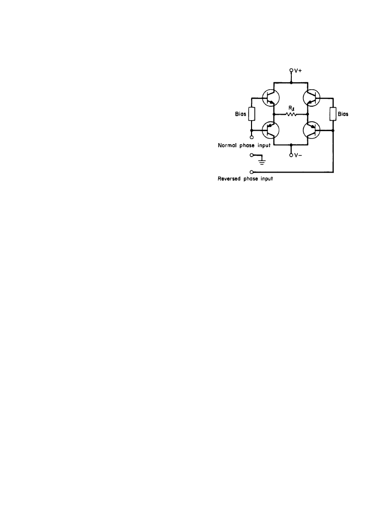
Full-bridge amplifiers are constructed by using two half-bridge amplifiers with the load con-
nected between the two output terminals and the two input terminals driven by signals of oppo-
site polarity from a phase inverter circuit (Figure 4.3.12). Peak voltage across the load then
becomes nearly equal to the total supply voltage, and peak-to-peak load voltage becomes nearly
twice the total supply voltage. This type of amplifier connection is preferred over the totem-pole-
transistor connection when high-voltage limitations of power devices restrict total available out-
put power into a fixed load resistance without using a transformer.
4.3.3
Classes of Amplifiers
Amplifiers are described as classes depending on the angle of conduction of signal current and
voltage-current relationships in the load.
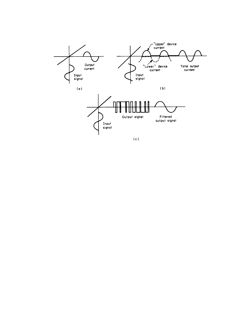
Class A amplifiers (Figure 4.3.13a) conduct signal current throughout the cycle of the signal
waveform. They have the lowest distortion before feedback and may be single-ended or push-
pull. An ideal Class A amplifier can have a sine-wave output efficiency not exceeding 50 percent
at full output.
Class B amplifiers (Figure 4.3.13b) conduct signal current exactly for one-half of the cycle of
the input-signal waveform. In a push-pull Class B amplifier, one device conducts for one half-
cycle, and the other device conducts for the remaining half-cycle. Linear Class B radio-fre-
quency amplifiers may have only one device, since the second-harmonic components are filtered
out in the narrowband matching network. An ideal Class B amplifier can have a maximum sine-
wave efficiency not exceeding 78 percent at full power output.
Figure 4.3.12
Full-bridge amplifier coupled to a
load.
Downloaded from Digital Engineering Library @ McGraw-Hill (www.digitalengineeringlibrary.com)
Copyright © 2004 The McGraw-Hill Companies. All rights reserved.
Any use is subject to the Terms of Use as given at the website.
Low Power Amplifiers

Low Power Amplifiers 4-61
Class AB amplifiers have a conduction angle between full conduction and half-cycle conduc-
tion and efficiencies between Classes A and B. Most conventional audio-frequency amplifiers
are adjusted in this way. As lower power outputs are needed with variations in signal amplitude,
the efficiency of Class A, AB, and B amplifiers will decrease proportionally to output voltage,
decreasing toward zero at very low output. When the load of such an amplifier is a reactive
impedance, such as a loudspeaker, efficiency will decrease still further, since any voltampere
energy sent to a reactance in one part of a cycle will be returned to the source and the resistance
in the circuit in the other part of the cycle.
Class C amplifiers conduct for less than one-half of a complete signal cycle. These amplifiers
are used primarily as radio-frequency amplifiers with the load tuned to the signal frequency.
Class D amplifiers (Figure 4.3.13c) are switching amplifiers using a high-frequency carrier
signal where the positive pulse on time is proportional to the modulation amplitude. The negative
pulse on time completes the rest of the cycle as with Class A amplifiers. In other designs, sepa-
rate circuits control positive and negative pulses as with Class B amplifiers. The load is isolated
from the amplifier output stage with a low-pass filter that does not consume the high-frequency
pulse energy. Class D amplifiers have a theoretical efficiency of 100 percent at all signal levels
but are difficult to design for wideband low-distortion operation because of the short switching
transition times required of the final high-power output stages and the difficulty of design of
feedback loops.
Class E amplifiers have as input signals rectangular pulses. The output load is tuned, but the
output voltage resembles a damped single pulse.
Figure 4.3.13
Output current as a function of input signal for amplifiers of various classes: (
a)
Class A, (
b) Class B, (c) Class D.
Downloaded from Digital Engineering Library @ McGraw-Hill (www.digitalengineeringlibrary.com)
Copyright © 2004 The McGraw-Hill Companies. All rights reserved.
Any use is subject to the Terms of Use as given at the website.
Low Power Amplifiers

4-62 Microphone Devices and Systems
There is no generally accepted agreement on naming amplifiers of classes above E. Several
types of amplifiers have been described with differing letters. These include amplifiers in which
several stages are connected in series, drawing power from several power supplies through isola-
tion diodes to provide output signal to a load. For small signals, only the stages connected to the
low-voltage supplies conduct current. As these stages saturate, the next stages then conduct cur-
rent from the next higher power supplies through the saturated stages into the load, and so on.
In a different version, a normal Class B amplifier obtains supply voltage from a high-effi-
ciency switching power supply, the output voltage of which is raised as output voltage demands
are increased. In all these amplifier designs attempts are made to improve efficiency with vary-
ing signal levels and with program-signal waveforms, which are nonsinusoidal.
4.3.4
Gain Block and the Operational Amplifier
A large number of audio- and video-frequency circuits are constructed by using operational
amplifiers because they permit these circuits to be designed with minimum complexity of com-
ponents. In most applications, the open-circuit voltage gain of an operational amplifier will be
much larger than the gain of the amplifier.
An amplifier gain block is matched to the output of the previous gain block or other circuit
when it is able to extract maximum power from the previous circuit. When the amplifier gain
block draws little current from the preceding circuit, the gain block is said to be bridged across
that circuit and must have a relatively high input impedance.
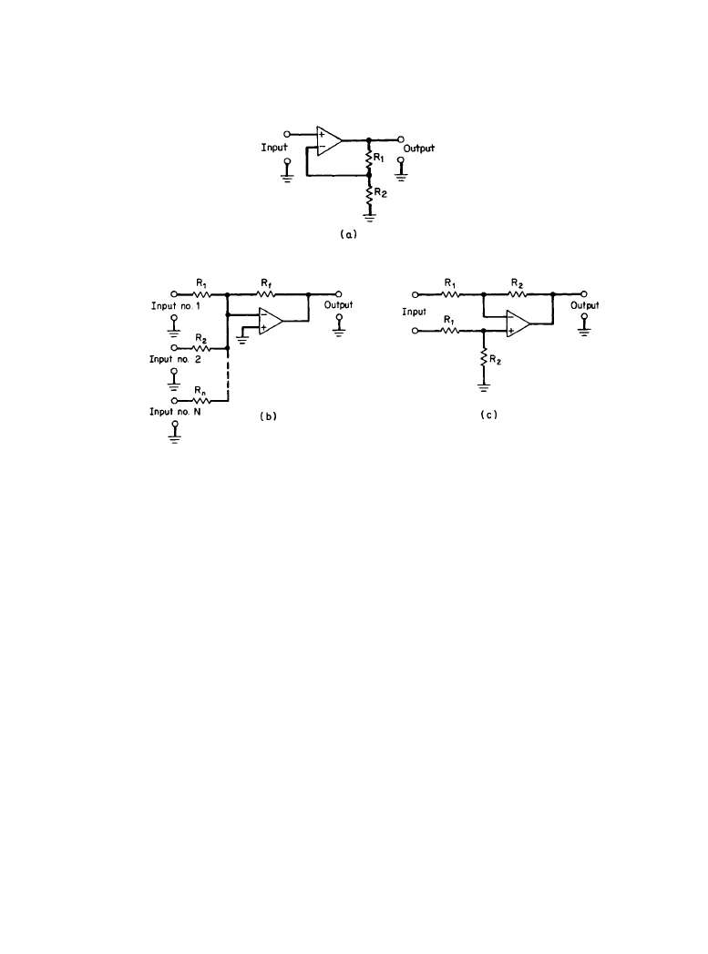
An operational amplifier connected as a noninverting amplifier can have a high input imped-
ance at its positive input while receiving feedback voltage from a voltage divider connected
between output and ground, with the voltage-divider junction connected to the negative input
(Figure 4.3.14a). The voltage gain is the voltage ratio of the divider.
An inverting operational amplifier can be used as a gain block, with the input resistor con-
nected between the source and the negative input and matching the desired load of the previous
stage. A feedback resistor connected between the output and the same negative input then sets
voltage gain equal to the ratio between the two resistors; the positive input is grounded (Figure
4.3.14b). Because there exists only a very low voltage at the negative input, several input resis-
tors can be connected between various input sources and the negative input. In this fashion, these
input signals can be mixed together with little danger of feedthrough between signals at each
source.
If resistance-capacitance networks are used in place of resistors, equalizer blocks can be
designed. With more complex networks, high-pass, low-pass, bandpass, and phase-shifting all-
pass blocks result.
These circuits make use of the common-ground mode and thus are unbalanced circuits. An
operational amplifier can also amplify the voltage difference between the two wires of a bal-
anced program line while having only little sensitivity to common-mode signals arriving in
phase, thereby reducing ground-loop voltages.
The simplest connection involves the use of two identical voltage-divider resistor pairs having
their junctions connected to the positive and negative inputs (Figure 4.3.14c). The input termi-
nals of the two networks are then connected to the two wires of the signal line. The return termi-
nal of the network connected to the positive input is grounded, and the other return terminal is
connected to the output of the operational amplifier. The differential voltage gain of such a cir-
Downloaded from Digital Engineering Library @ McGraw-Hill (www.digitalengineeringlibrary.com)
Copyright © 2004 The McGraw-Hill Companies. All rights reserved.
Any use is subject to the Terms of Use as given at the website.
Low Power Amplifiers

Low Power Amplifiers 4-63
cuit is equal to the ratio of the resistance values, while the common-mode gain is limited by resis-
tor accuracy and the residual errors of the operational amplifier, and particularly its common-
mode rejection. The input impedances of the positive and negative inputs to the circuit are not
equal. A number of gain blocks can be interconnected to become a more complex amplifier sys-
tem [8].
4.3.4a
Feedback and Feed Forward
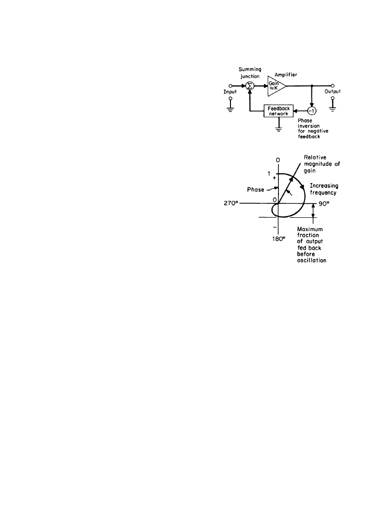
Feedback is the return of a fraction of the output signal to the input (Figure 4.3.15). The returned
fraction is added to the input signal at the feedback node in the feedback loop of the system. The
input signal to the system with feedback for the same output as before feedback is now the vector
sum of the original input signal and the feedback signal. Feedback is negative when the new
required input signal is larger than the signal without feedback and positive when it is smaller.
Feedback may be acoustic, mechanical, or electronic, depending upon the type of signal
amplified. In amplifiers for audio- and video-frequency signals the feedback signal is usually a
portion of the output voltage or output current. When the returned fraction is negative and is
obtained through a linear network, the reduction ratio of amplifier errors, such as distortion or
phase shift, is proportional to the reduction in amplifier gain due to feedback. In the limit, with
Figure 4.3.14
Operational amplifier circuits: (
a) the gain-block voltage gain = (1 +R
1
/
R
2
) with the
same polarity of the input and output signals, (
b) the gain-block voltage gain = (R
f
/
R
1
), 1 (
R
f
/
R
2
) or
– (
R
f
/
R
n
) with opposite polarity of input and output signals, (
c) the gain-block differential voltage
gain = (
R
2
/
R
1
) and low common-mode gain, limited by resistor matching and loop gain.
Downloaded from Digital Engineering Library @ McGraw-Hill (www.digitalengineeringlibrary.com)
Copyright © 2004 The McGraw-Hill Companies. All rights reserved.
Any use is subject to the Terms of Use as given at the website.
Low Power Amplifiers

4-64 Microphone Devices and Systems
very high amplifier gain before feedback, the response of the amplifier with respect to frequency
will nearly equal the reciprocal of the loss of the feedback network as measured from output to
input [9].
Linear Feedback
Linear feedback exists when the feedback signal is only a level-independent portion of the output
signal. Negative feedback cannot be applied in ever-increasing amounts because all amplifiers
have increasing amounts of phase shift as the limits of the frequency range are approached, par-
ticularly at high frequencies (Figure 4.3.16). Whenever phase shift of the feedback signal is
between 90 and 270° of phase with respect to the input signal at the feedback node, amplification
with feedback will be greater with feedback than without. In the limit, no more positive feedback
signal than the original input signal can be returned to the amplifier input before oscillation
starts at the frequency where the returned feedback signal is equal to the original input signal in
both amplitude and phase. This condition is desirable only in oscillators, not in amplifiers.
Another reason for using little negative feedback is that some intermediate stage of the ampli-
fier may current-limit feeding a capacitor before the output stage is overloaded by input signals.
This distortion is known as slew-rate limiting and is a cause of transient intermodulation distor-
tion.
Figure 4.3.15
Negative-feedback amplifier. Voltage
gain =
K/[1 + (Kb)], where K = amplifier voltage gain
without feedback and
b = gain of the feedback net-
work, usually 1 on less.
Figure 4.3.16
Polar plot of amplifier gain and phase
from dc relative to frequency. At higher frequencies,
a negative component of the gain characteristics
limits the maximum usable feedback before oscilla-
tion occurs.
Downloaded from Digital Engineering Library @ McGraw-Hill (www.digitalengineeringlibrary.com)
Copyright © 2004 The McGraw-Hill Companies. All rights reserved.
Any use is subject to the Terms of Use as given at the website.
Low Power Amplifiers