ВУЗ: Казахская Национальная Академия Искусств им. Т. Жургенова
Категория: Книга
Дисциплина: Не указана
Добавлен: 03.02.2019
Просмотров: 21697
Скачиваний: 19

6-46 Digital Coding of Audio Signals
6.4.3d
Example DSP Device
The functional description of a representative DSP device will help to illustrate the concepts out-
line previously in this chapter. Table 6.4.1 lists the overall characteristics for members of the
TMS320C55x generation of fixed-point digital signal processors (Texas Instruments). Features
for the high performance, low-power C55x CPU include the following [2]:
•
Advanced multiple-bus architecture with one internal program memory bus and five internal
data buses (three dedicated to reads and two dedicated to writes)
•
Unified program/data memory architecture
Table 6.4.1 Characteristics of the TMS320C55x Processors
(
After [2]. Courtesy of Texas
Instruments.)
Parameter
VC5510
Memory
On-chip SARAM
32 K words (64 K bytes)
On-chip DARAM
128 K words (256 K bytes)
On-chip ROM
16 K words (32 K bytes)
Total addressable memory (internal/external)
8M words (16 M bytes)
On-chip bootloader (in ROM)
Yes
Peripherals
McBSPs
3
DMA controller
Yes
EHPI (16-bit)
Yes
Configurable instruction cache
24K bytes
Timers
2
Programmable DPLL clock generator
Yes
General Purpose I/O Pins
Dedicated input/output
Yes
XF—dedicated output
1
Multiplexed with McBSP (input/output)
21
Multiplexed with timer (output only)
2
CPU Cycle Time/Speed
160 MHz (6.25 ns)
Yes
200 MHz (5 ns)
Yes
Package Type
240-pin BGA
Downloaded from Digital Engineering Library @ McGraw-Hill (www.digitalengineeringlibrary.com)
Copyright © 2004 The McGraw-Hill Companies. All rights reserved.
Any use is subject to the Terms of Use as given at the website.
DSP Devices and Systems

DSP Devices and Systems 6-47
•
Dual 17-bit
× 17-bit multipliers coupled to 40-bit dedicated adders for non-pipelined single-
cycle multiply accumulate (MAC) operations
•
Compare, select, and store unit (CSSU) for the add/compare section of the Viterbi operator
•
Exponent encoder to compute an exponent value of a 40-bit accumulator value in a single
cycle
•
Two address generators with eight auxiliary registers and two auxiliary register arithmetic
units
•
Data buses with bus holders
•
8 M
× 16-bit (16 Mbyte) total addressable memory space
•
Single-instruction repeat or block repeat operations for program code
•
Conditional execution
•
Seven-stage pipeline for high instruction throughput
•
Instruction buffer unit that loads, parses, queues, and decodes instructions to decouple the
program fetch function from the pipeline
•
Program flow unit that coordinates program actions among multiple parallel CPU functional
units
•
Address data flow unit that provides data address generation and includes a 16-bit arithmetic
unit capable of performing arithmetic, logical, shift, and saturation operations
•
Data computation unit containing the primary computation units of the CPU, including a 40-
bit arithmetic logic unit, two multiply-accumulate units, and a shifter
Because many DSP chips are used in portable systems, power consumption is a key operating
parameter. As a result, power control features are an important DSP specification. Hardware and
software functions designed to conserve power include:
•
Software-programmable idle domains that provide configurable low-power modes
•
Automatic power management
•
Advanced low-power CMOS process
Functional Overview
The C55x architecture achieves power-efficient performance through increased parallelism and a
focus on reduction in power dissipation. The CPU supports an internal bus structure composed
of the following elements [2]:
•
One program bus
•
Three data read buses
•
Two data write buses
•
Additional buses dedicated to peripheral and DMA activity
These buses provide the ability to perform up to three data reads and two data writes in a single
cycle. In parallel, the DMA controller can perform up to two data transfers per cycle independent
Downloaded from Digital Engineering Library @ McGraw-Hill (www.digitalengineeringlibrary.com)
Copyright © 2004 The McGraw-Hill Companies. All rights reserved.
Any use is subject to the Terms of Use as given at the website.
DSP Devices and Systems

6-48 Digital Coding of Audio Signals
of CPU activity. The C55x CPU provides two multiply-accumulate units each capable of 17-bit
× 17-bit multiplication in a single cycle. A central 40-bit arithmetic/logic unit (ALU) is sup-
ported by an additional 16-bit ALU. Use of ALUs is subject to instruction set control. This pro-
grammability provides the capacity to optimize parallel activity and power consumption. These
resources are managed in the address data flow unit (AU) and data computation unit (DU) of the
C55x CPU.
The C55x architecture supports a variable byte width instruction set for improved code den-
sity. The instruction buffer unit (IU) performs 32-bit program fetches from internal or external
memory and queues instructions for the program unit (PU). The program unit decodes the
instructions, directs tasks to AU and DU resources, and manages the fully-protected pipeline.
A configurable instruction cache is also available to minimize external memory accesses,
improving data throughput and conserving system power.
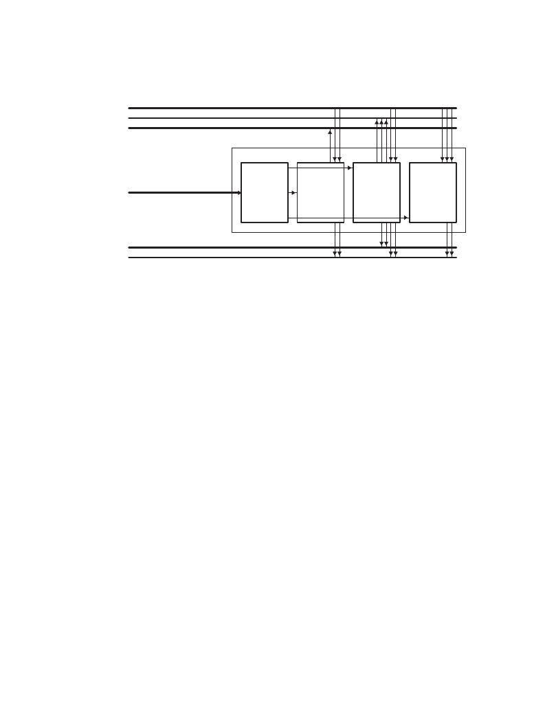
The C55x architecture is built around four primary blocks:
•
The instruction buffer unit
•
Program flow unit
•
Address data flow unit
•
Data computation unit
These functional units exchange program and data information with each other and with memory
through multiple dedicated internal buses. Figure 6.4.11 shows the principal blocks and bus
structure in the C55x devices.
Program fetches are performed using the 24-bit program address bus (PAB) and the 32-bit
program read bus (PB). The functional units read data from memory via three 16-bit data read
buses named B-bus (BB), C-bus (CB), and D-bus (DB). Each data read bus also has an associ-
CPU
Program Read Bus PB (32)
Data Write Buses EB, FB (2x16)
Data Write Address Buses EAB, FAB (2x24)
Program Address Bus PAB (24)
Data Read Address Buses BAB, CAB, DAB (3x24)
Data Read Buses BB, CB, DB (3x16)
(DU)
Unit
Computation
Data
(IU)
Unit
Buffer
Instruction
(PU)
Unit
Flow
Program
(AU)
Unit
Flow
Data
Address
Figure 6.4.11
Functional Block Diagram of the TMS320C55x DSP series. (
From [2]. Courtesy of
Texas Instruments.)
Downloaded from Digital Engineering Library @ McGraw-Hill (www.digitalengineeringlibrary.com)
Copyright © 2004 The McGraw-Hill Companies. All rights reserved.
Any use is subject to the Terms of Use as given at the website.
DSP Devices and Systems

DSP Devices and Systems 6-49
ated 24-bit data read address bus (BAB, CAB, and DAB). Single operand reads are performed on
the D-bus. Dual-operand reads use C-bus and D-bus. B-bus provides a third read path and can be
used to provide coefficients for dual-multiply operations.
Program and data writes are performed on two 16-bit data write buses called E-bus (EB) and
F-bus (FB). The write buses also have associated 24-bit data write address buses (EAB and
FAB). Additional buses are present on the C55x devices to provide dedicated service to the
DMA controller and the peripheral controller.
All C55x DSP devices use the same CPU structure but are capable of supporting different on-
chip peripherals and memory configurations. The on-chip peripherals include:
•
Digital phase-locked loop (DPLL) clock generation
•
Instruction cache
•
External memory interface (EMIF)
•
Direct memory access (DMA) controller
•
16-bit enhanced host port interface (EHPI)
•
Multichannel serial ports (McBSPs)
•
16-bit timers with 4-bit prescalers
•
General-purpose I/O (GPIO) pins
•
Trace FIFO (for emulation purposes only)
Interface
SDRAM
Interface
Bus Hold
Interface
SBSRAM
Interface
Asynchronous
Interfaces
All External
Shared by
Bus
Program
CPU
Buses
Data
CPU
Controller†
Peripheral Bus
Controller
DMA
CLKMEM‡
SDA10
SDWE
SDCAS
SDRAS
HOLDA
HOLD
SSWE
SSOE
SSADS
ARE
AWE
AOE
ARDY
BE[3:0]
CE[3:0]
A[21:0]
D[31:0]
32-bit EMIF
Internal Units of C55x
External Memory
† This connection allows the CPU to access the EMIF registers.
‡ The CLKMEM signal is shared by the SDRAM and SBSRAM interfaces.
Figure 6.4.12
Block diagram of EMIF for the TMS320C55x DSP. (
From [2]. Courtesy of Texas
Instruments.)
Downloaded from Digital Engineering Library @ McGraw-Hill (www.digitalengineeringlibrary.com)
Copyright © 2004 The McGraw-Hill Companies. All rights reserved.
Any use is subject to the Terms of Use as given at the website.
DSP Devices and Systems

6-50 Digital Coding of Audio Signals
Peripheral control registers are mapped to an I/O space separate from the main memory
space. The peripheral bus controller handles exchange of data between peripherals and the CPU
via dedicated peripheral buses.
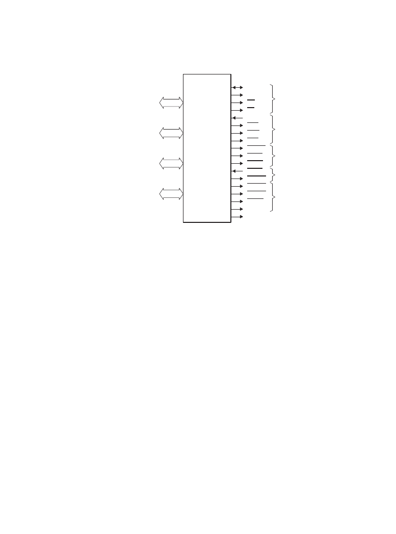
The EMIF supports a “glueless” interface from the C55x to a variety of external memory
devices. For each memory type, the EMIF supports 8-bit, 16-bit, and 32-bit accesses for both
reads and writes. For writes, the EMIF controls the byte enable signals and the data bus to per-
form 8-bit transfers or 16-bit transfers. For reads, the entire 32-bit bus is read. Then, it is inter-
nally parsed by the EMIF. The EMIF block diagram, Figure 6.4.12, shows the interface between
external memory and the internal resources of the C55x.
6.4.4
References
1.
Pohlmann, Ken: Principles of Digital Audio, McGraw-Hill, New York, N.Y., 2000.
2.
TMS320C55x DSP Functional Overview, Texas Instruments, Dallas, TX, literature No.
SRPU312, June 2000.
Downloaded from Digital Engineering Library @ McGraw-Hill (www.digitalengineeringlibrary.com)
Copyright © 2004 The McGraw-Hill Companies. All rights reserved.
Any use is subject to the Terms of Use as given at the website.
DSP Devices and Systems