ВУЗ: Казахская Национальная Академия Искусств им. Т. Жургенова
Категория: Книга
Дисциплина: Не указана
Добавлен: 03.02.2019
Просмотров: 21694
Скачиваний: 19

DSP Devices and Systems 6-41
only if all its poles are inside the unit circle of the z-plane. Zeros can lie anywhere. When all
zeros lie inside the unit circle, the system is called a minimum-phase network. If all poles are
inside the unit circle and all zeros are outside, and if poles and zeros are always reflections of one
another in the unit circle, the system is a constant-amplitude, or all-pass network. If a system has
zeros only, except for the origin, and they are reflected in pairs in the unit circle, the system is
phase linear. No real function can have more zeros than poles. When the coefficients are real,
poles and zeros occur in complex conjugate pairs; their plot is symmetrical across the real z-axis.
The closer its location to the unit circle, the greater the effect of each pole and zero on frequency
response.
6.4.3
DSP Elements
Successful DSP applications require sophisticated hardware and software [1]. However, all DSP
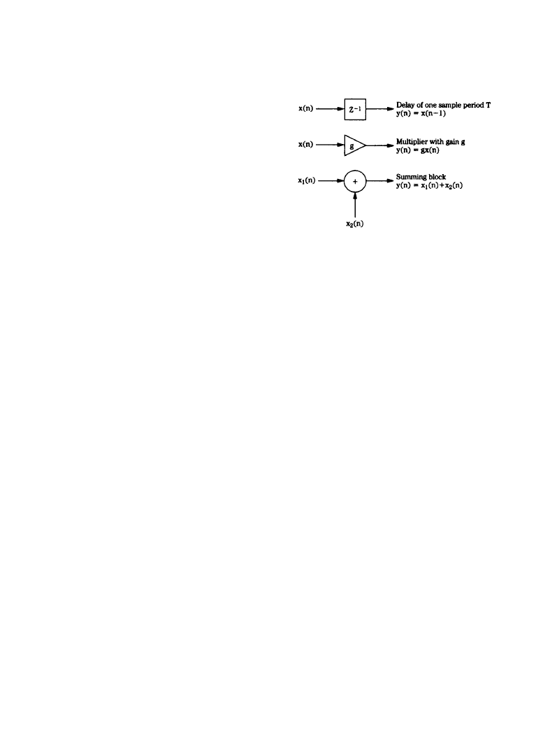
processing can be considered in three basic processing operations (Figure 6.4.7):
•
Summing, where multiple digital values are added to produce a single result.
•
Multiplication, where a gain change is accomplished by multiplying the sample value by a
coefficient.
•
Time delay, where a digital value is stored for one sample period (n – 1).
The delay element (realized with shift registers or memory locations) is alternatively notated as
z
–1
because a delay of one sampling period in the time domain corresponds to multiplication by
z
–1
in the z-domain; thus z
–1
x(n) = x(n – 1). Delays can be cascaded, for example, a z-
2
term
describes a two-sample (n - 2) delay. Although it is usually most convenient to operate with sam-
ple numbers, the time of a delay can be obtained by taking nT, where T is the sampling interval.
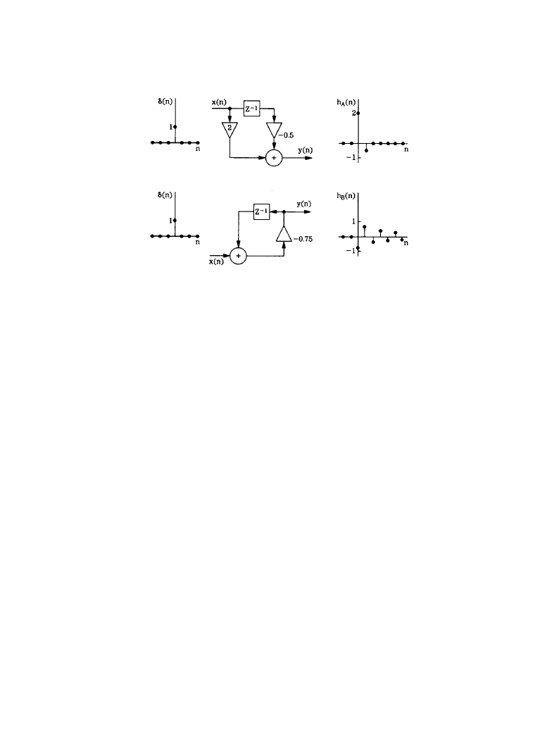
Figure 6.4.8 shows two examples of simple networks and their impulse responses. LTD systems
such as these are completely described by the impulse response.
In practice, these elemental operations are performed many times for each sample, in specific
configurations depending on the desired result. In this way, algorithms can be devised to perform
operations useful to signal processing, such as reverberation, equalization, data compression,
limiting, and noise removal. Of course, for real-time operation, all processing for each sample
must be completed within one sampling period.
Figure 6.4.7
The three basic elements in any
DSP system: delay, multiplication, and summa-
tion. (
From [1]. Used with permission.)
Downloaded from Digital Engineering Library @ McGraw-Hill (www.digitalengineeringlibrary.com)
Copyright © 2004 The McGraw-Hill Companies. All rights reserved.
Any use is subject to the Terms of Use as given at the website.
DSP Devices and Systems

6-42 Digital Coding of Audio Signals
6.4.3a
Sources of Errors
In general, errors in digital processors can be classified as coefficient errors, limit cycle errors,
overflow, truncation, and round-off errors [1]. Coefficient errors occur when a coefficient is not
specified with sufficient accuracy. Limit cycle error might occur when a signal is removed from
a filter, leaving a decaying sum. This decay might become zero or might oscillate at a constant
amplitude, known as limit cycle oscillation. This effect can be eliminated, for example, by offset-
ting the filter output so that truncation always produces a zero output. Overflow occurs when a
register length is exceeded, resulting in a computational error. In the case of wrap-around, when a
1 is added to the maximum value positive two’s complement number, the result is the maximum
value negative number. In short, the information has overflowed into a nonexistent bit. To pre-
vent this, saturating arithmetic can be used so that when the addition of two positive numbers
would result in a negative number, the maximum positive sum is substituted instead.
Truncation and round-off errors occur whenever the word length of a computed result is lim-
ited. Errors accumulate both inside the processor during calculation, and when word length is
reduced for output through a D/A converter. However, A/D conversion always results in quanti-
zation error, and computation error can appear in different guises. For example, when two n-bit
numbers are multiplied, the number of output bits will be 2n – 1. Thus, multiplication almost
doubles the number of bits required to represent the output. Although many hardware multipliers
can perform double precision computation, a finite word length must be maintained following
multiplication, thus limiting precision. Discarded data results in an error that is analogous to A/D
quantization. To be properly modeled, multiplication must be followed by quantization. Multipli-
cation does not introduce error, but inability to keep the extra bits does.
Rather than truncate a word—for example, following multiplication—the value can be
rounded; that is, the word is taken to the nearest available value. This results in a peak error of 1/
2 LSB, and a RMS value of 1/(12)
1/2
, or 0.288 LSB. This round-off error will accumulate over
successive calculations. In general, the number of calculations must be large for significant error.
(
a)
(
b)
Figure 6.4.8
LTD systems can be characterized by their impulse responses: (
a) simple nonrecur-
sive system and its impulse response, (
b) simple recursive system and its impulse response. (van
den Enden and Verhoeckx. From [1]. Used with permission.)
Downloaded from Digital Engineering Library @ McGraw-Hill (www.digitalengineeringlibrary.com)
Copyright © 2004 The McGraw-Hill Companies. All rights reserved.
Any use is subject to the Terms of Use as given at the website.
DSP Devices and Systems

DSP Devices and Systems 6-43
However, in addition, dither information can be lost during computation. For example, when a
properly dithered 16-bit word is input to a 32-bit processor, even though computation is of high
precision, the output signal can be truncated to 16 bits for conversion through the output D/A
converter. For example, a 16-bit signal that is delayed and scaled by a 12-dB attenuation would
result in a 12-bit undithered signal. To overcome this, digital dithering to the resolution of the
next processing step should be used in a computation.
6.4.3b
DSP Integrated Circuits
A DSP chip is a specialized hardware device that performs digital signal processing under the
control of software algorithms [1]. DSP chips are stand-alone processors, often independent of
host CPUs (central processing units), and are specially designed for operations used in spectral
and numerical applications. For example, large numbers of multiplications are possible, as well
as special addressing modes such as bit-reverse and circular addressing. When the memory and
input/output circuits are added, the result is an integrated digital signal processor. Such a general-
purpose DSP chip is software programmable, and thus can be used for a variety of signal-pro-
cessing applications. Alternatively, a custom signal processor can be designed to accomplish a
specific task.
DSP chips are designed according to two arithmetic types, fixed integer and floating point,
which define the format of the data they operate on. A fixed integer chip uses two’s complement,
binary integer data. Floating point chips use integer and floating point numbers (represented as a
mantissa and exponent). The dynamic range of a fixed integer chip is based on its word length;
data must be scaled to prevent overflow; this can increase programming complexity. The scien-
tific notation used in a floating point chip allows larger dynamic range, without overflow prob-
lems. However, the resolution of floating point representation is limited by the word length of the
exponent.
DSP chips often use a pipelining architecture so that several instructions can be paralleled.
For example, a fetch (fetch instruction from memory and update program counter), decode
(decode instruction and generate operand address), read (read operand from memory), and exe-
cute (perform necessary operations) can be effectively executed in one clock cycle with pipelin-
ing. A pipeline manager, aided by proficient user programming, helps ensure rapid processing.
DSP chips, like all computers, are comprised of input and output devices, an arithmetic unit, a
control unit, and memory, interconnected by buses. All computers originally used a single
sequential bus (von Neumann architecture), shared by data, memory addresses, and instructions.
However, in a DSP chip a particularly large number of operations must be performed quickly for
real-time operation. Thus, parallel bus structures are used (such as the Harvard architecture) that
store data and instructions in separate memories and transfers them via separate buses. For
example, a chip can have separate buses for program, data, and DMA, providing parallel pro-
gram fetches, data reads, as well as DMA operations with slower peripherals.
General purpose DSP chips tend to follow a similar architecture; typical elements include the
following:
•
Multiply-accumulate unit
•
Data address generator
•
Data RAM
•
Coefficient RAM
Downloaded from Digital Engineering Library @ McGraw-Hill (www.digitalengineeringlibrary.com)
Copyright © 2004 The McGraw-Hill Companies. All rights reserved.
Any use is subject to the Terms of Use as given at the website.
DSP Devices and Systems

6-44 Digital Coding of Audio Signals
•
Coefficient address generator
•
Program control unit
•
Program ROM
These components are connected by the following buses:
•
The data bus
•
Coefficient bus
•
Control bus
6.4.3c
DSP Applications
In addition to digital filtering, some of the most powerful and creative applications of digital sig-
nal processing come in the form of specialized processing of audio and video signals. Building
on the basic operations of multiplication and delay, sophisticated operations can be developed.
Reverberation perhaps epitomizes the degree of time manipulation possible in the digital
domain; it is possible to synthesize reverberation to both simulate natural acoustical environ-
ments and to create acoustical environments that could not physically exist.
Digital Delay
A delay block is a simple storage unit, such as a memory location [1]. A sample is placed in
memory, stored, then recalled some time later and output. A delay unit can be described by the
equation y(n) = x(n – m) where m is the delay in samples. Generally, when the delay is small, the
frequency response of the signal is altered; when the delay is longer, an echo results. Just as in
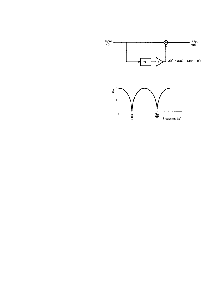
filtering, a simple delay can be used to create sophisticated effects. For example, Figure 6.4.9a
Figure 6.4.9
A delay block can be
used to create an echo circuit: (
a)
the circuit contains an
mT delay
and gain stage, (
b) with shorter
delay times, a comb filter response
will result. (
Bloom, Berkhout, and
Eggermont. From [1]. Used with
permission.)
(
a)
(
b)
Downloaded from Digital Engineering Library @ McGraw-Hill (www.digitalengineeringlibrary.com)
Copyright © 2004 The McGraw-Hill Companies. All rights reserved.
Any use is subject to the Terms of Use as given at the website.
DSP Devices and Systems

DSP Devices and Systems 6-45
shows an echo circuit using a delay block. Delay mT is of duration m samples, and samples are
multiplied by a gain coefficient (a scaling factor) less than unity. If the delay time is set between
10 and 50 ms, an echo results; with shorter fixed delays, a comb filter response results, as shown
in Figure 6.4.9b. Peaks and dips are equally spaced through the frequency response from 0 Hz to
the Nyquist frequency. The number of peaks depends on the delay time; the longer the delay, the
more peaks.
A comb filter can be either recursive or nonrecursive. It cascades a series of delay elements,
creating a new response. Mathematically, a nonrecursive comb filter can be designed by adding
the input sample to the same sample but delayed
(6.4.11
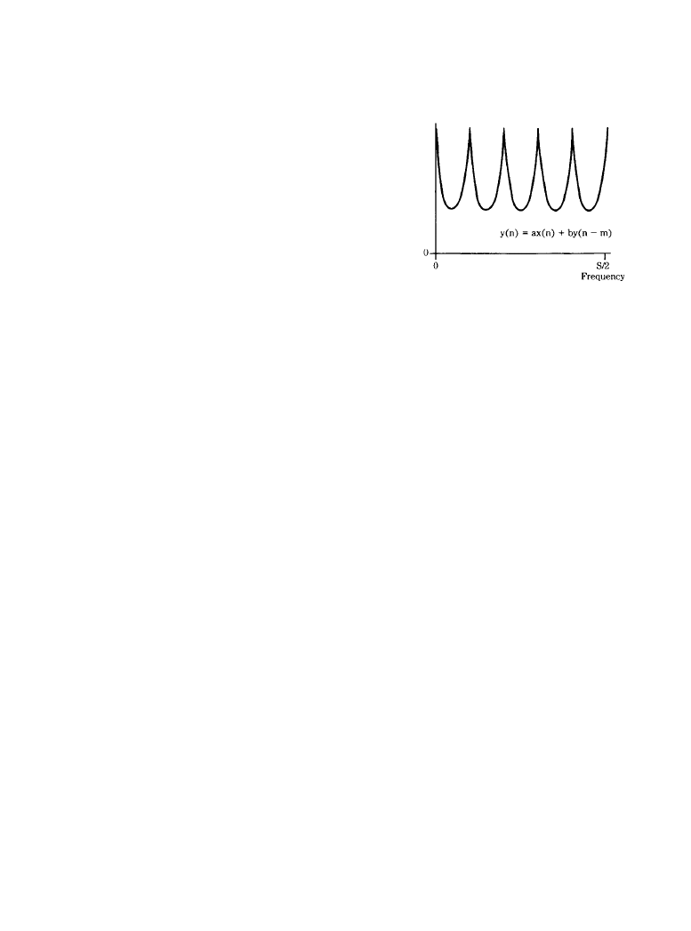
where m is the delay time in samples. A recursive comb filter creates a delay with feedback. The
delayed signal is attenuated and fed back into the delay
(6.4.12)
This yields a response as shown in Figure 6.4.10. The number of peaks depends on the duration
of the delay; the longer the delay, the greater the number of peaks.
An all-pass filter is one that has a flat frequency response from 0 Hz to the Nyquist frequency.
However, its phase response causes different frequencies to be delayed by different amounts. An
all-pass filter can be described as
(6.4.13)
If the delay in the foregoing circuits is replaced by a digital all-pass filter or a cascade of all-
pass filters, a phasing effect is achieved
(6.4.14)
The effect becomes more pronounced as the delay increases. The system exhibits nonuniformly
spaced notches in its frequency response, varying independently in time.
y n
( )
x n
( ) ax n m
–
(
)
+
=
y n
( )
ax n
( ) by n m
–
(
)
+
=
y n
( )
ax n
( )
–
x n
1
–
(
) by n 1
–
(
)
+
+
=
y n
( )
ax n
( )
–
x n
m
–
(
) by n m
–
(
)
+
+
=
Figure 6.4.10
A recursive comb filter creates a delay
with feedback, yielding a toothed frequency response.
(
From [1]. Used with permission.)
Downloaded from Digital Engineering Library @ McGraw-Hill (www.digitalengineeringlibrary.com)
Copyright © 2004 The McGraw-Hill Companies. All rights reserved.
Any use is subject to the Terms of Use as given at the website.
DSP Devices and Systems