ВУЗ: Казахская Национальная Академия Искусств им. Т. Жургенова
Категория: Учебное пособие
Дисциплина: Не указана
Добавлен: 03.02.2019
Просмотров: 17360
Скачиваний: 18

Amplifier and loudspeaker protection
An alternative approach drops out the DC protection relay when overload
is detected. The relay may either be opened for a few seconds delay, after
which it resets, or stay latched open until the protection circuit is reset. This
is normally done by cycling the mains power on and off, to avoid the
expense of a reset button that would rarely be used.
If the equipment is essentially operated unattended, so that an overload
condition may persist for some time, the self-resetting system will subject
the output semiconductors to severe temperature changes, which may
shorten their operational lifetime.
Plotting the protection locus
The standard method of representing the conditions experienced by output
devices, of whatever technology, is to draw loadlines onto a diagram of the
component’s SOA, to determine where they cross the limits of the area.
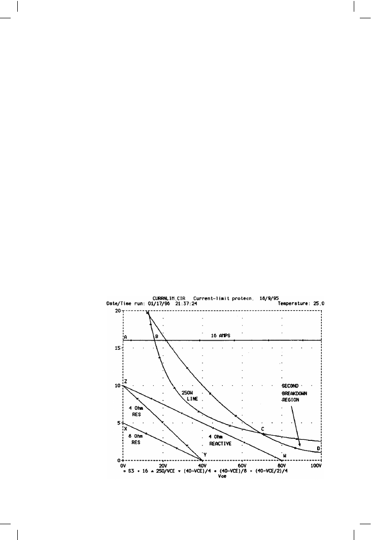
This is shown in Figure 13.1, for an amplifier with +/–40 V HT rails, which
would give 100 W into 8 ! and 200 W into 4 !, ignoring losses; the power
transistor is a Motorola MJ15024. You do not need to fix the HT voltage
before drawing most of the diagram; the position of the SOA limits is fixed
by the device characteristics. The line AB represents the maximum current
rating of 16 A, and the reciprocal curve BC the maximum power dissipation
of 250 W. The maximum Vce is 250 V, and so is far off the diagram to the
right. Line CD defines the second-breakdown region, effectively an extra
375
Figure 13.1
The Safe Operating
Area (SOA) of a
typical TO3 high-
power transistor, in
this case the Motorola
MJ15024

Audio Power Amplifier Design Handbook
area removed from the high-voltage end of the power-limited region.
Second-breakdown is an instability phenomenon that takes a little time to
develop, so manufacturer’s data often allows brief excursions into the
region between the second-breakdown line and the power limit. The
nearer these excursions go towards the power limit, the briefer they must be
if the device is to survive, and trying to exploit this latitude in amplifiers is
living dangerously, because the permitted times are very short (usually tens
of microseconds) compared with the duration of audio waveforms.
The resistive loadline XY represents an 8 ! load, and as a point moves
along it, the co-ordinates show the instantaneous voltage across the output
device and the current through it. At point X, the current is maximal at 5.0 A
with zero voltage across the device, as Vce(sats) and the like can be ignored
without significant error. The power dissipated in the device is zero, and
what matters is that point X is well below the current-limit line AB. This
represents conditions at clipping.
At the other end, at Y, the loadline has hit the X-axis and so the device
current is zero, with one rail voltage (40 V) across it. This represents the
normal quiescent state of an amplifier, with zero volts at its output, and zero
device dissipation once more. So long as Y is well to the left of the
maximum-voltage line all is well. Note that while you do not need to
decide the HT voltage when drawing the SOA for the device, you must do
so before the loadlines are drawn, as all lines for purely resistive loads
intersect the X-axis at a voltage representing one of the HT rails.
Intermediate points along XY represent instantaneous output voltages
between 0 V and clipping; voltage and current co-exist and so there is
significant device dissipation. If the line cuts the maximum-power rating
curve BC, the dissipation is too great and the device will fail.
Different load resistances are represented by lines of differing slope; ZY is
for a 4 ! load. The point Y must be common to both lines, for the current
is zero and the rail voltage unchanged no matter what load is connected to
a quiescent amplifier. Point Z is however at twice the current, and there is
clearly a greater chance of this low-resistance line intersecting the power
limit BC. Resistive loads cannot reach the second-breakdown region with
these rails.
Unwelcome complications are presented by reactive loading. Maximum
current no longer coincides with the maximum voltage, and vice-versa. A
typical reactive load turns the line XY into an ellipse, which gets much
nearer to the SOA limit. The width (actually the minor axis, to be
mathematical) of the ellipse is determined by the amount of reactance
involved, and since this is another independent variable, the diagram could
soon become over-complex. The solution is to take the worst-case for all
possible reactive loads of the form R+jX, and instead of trying to draw
hundreds of ellipses, to simply show the envelope made up of all their
closest approaches to the SOA limit. This is another straight line, drawn
from the same maximum current point Z to a point W at twice the rail
376

Amplifier and loudspeaker protection
voltage. There is clearly a much greater chance that the ZW line will hit the
power-limit or second-breakdown lines than the 4 ! resistive line ZY, and
the power devices must have an SOA large enough to give a clear safety
margin between its boundary and the reactive envelope line for the lowest
rated load impedance. The protection locus must fit into this gap, so it must
be large enough to allow for circuit tolerances.
The final step is plot the protection locus on the diagram. This locus, which
may be a straight line, a series of lines, or an arbitrary curve, represents the
maximum possible combinations of current and voltage that the protection
circuitry permits to exist in the output device. Most amplifiers use some
form of VI limiting, in which the permitted current reduces as the voltage
across the device increases, putting a rough limit on device power
dissipation. When this relationship between current and voltage is plotted,
it forms the protection locus.
This locus must always be above and to the right of the reactive envelope
line for the lowest rated load, or the power output will be restricted by the
protection circuitry operating prematurely. It must also always be to the left
and below the SOA limit, or it will allow forbidden combinations of voltage
and current that will cause device failure.
Simple current-limiting
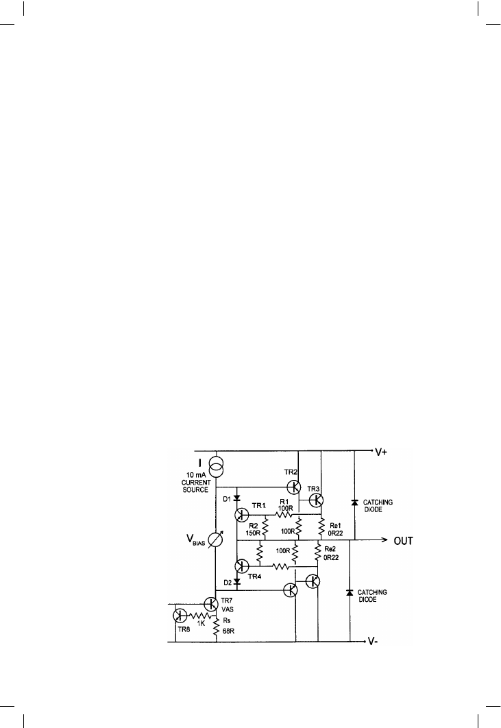
The simplest form of overload protection is shown in Figure 13.2, with both
upper and lower sections shown. For positive output excursions, R1
samples the voltage drop across emitter-resistor Re1, and when it exceeds
the Vbe of approx. 0.6 V, TR1 conducts and shunts current away from TR2
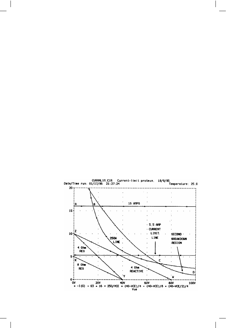
base. The component values in Figure 13.2 give a 5.5 A constant-current
377
Figure 13.2
Simple current-limit
circuit

Audio Power Amplifier Design Handbook
regime as shown in Figure 13.3, which was simulated using a model like
Figure 13.8 below. The loadlines shown represent 8 ! and 4 ! resistive,
and 4 ! worst-case reactive (ZW). The current-limit line is exactly
horizontal, though it would probably show a slight slope if the simulation
was extended to include more of the real amplifier, such as real current
sources, etc.
The value of Re1 is usually determined by the requirements of efficiency or
quiescent stability, and so the threshold of current-limiting is set by R1 and
R2. This circuit can only operate at a finite speed, and so R1 must be large
enough to limit TR1 base current to a safe value. 100 ! seems sufficient in
practice. Re1 is usually the output emitter resistor, as well as current sensor,
and so does double duty.
The current drawn by TR1 in shunting away TR2 base drive is inherently
limited by I, the constant-current load of the VAS. There is no such limit
on TR4, which can draw large and indeterminate currents through VAS
transistor TR7. If this is a TO-92 device it will probably fail. It is therefore
essential to limit the VAS current in some way, and a common approach
is shown in Figure 13.2. There is now a secondary layer of current-
limiting, with TR8 protecting TR7 in the same way that TR1 protects TR2,
3. The addition of Rs to sense the VAS current does not significantly affect
VAS operation, and does not constitute local negative feedback. This is
because the input to TR7 is a current from the input stage, and not a
378
Figure 13.3
Current-limiting with
+/–40 V HT rails

Amplifier and loudspeaker protection
voltage; the development of a voltage across Rs does not affect the value
of this current, as it is effectively being supplied from a constant-current
source.
It has to be faced that this arrangement often shows signs of HF instability
when current limiting, and this can prove difficult or impossible to
eradicate completely. (This applies to single and double-slope VI limiting
also.) The basic cause appears to be that under limiting conditions there are
two feedback systems active, each opposing the other. The global voltage
feedback is attempting to bring the output to the demanded voltage level,
while the overload protection must be able to override this to safeguard the
output devices. HF oscillation is often a danger to BJT output devices, but
in this case it does not seem to adversely affect survivability. Extensive tests
have shown that in a conventional BJT output stage, the oscillation seems
to reduce rather than increase the average current through the output
devices, and it is arguable that it does more good than harm. It has to be
said, however, that the exact oscillation mechanism remains obscure
despite several investigations, and the state of our knowledge in this area is
far from complete.
The diodes D1, D2 in the collectors of TR1, TR4 prevent them conducting
in the wrong half cycle if the Re voltage drops are large enough to make the
collector voltage go negative. Under some circumstances you may be able
to omit them, but the cost saving is negligible.
The loadline for an output short-circuit on the SOA plot is a vertical line,
starting upwards from Y, the HT rail voltage on the X-axis, and
representing that current increases indefinitely without any reduction of
the voltage drop across the output devices. An example is shown in
Figure 13.3 for +/–40 V rails. When the short-circuit line is prolonged
upwards it hits the 5.5 A limiting locus at 40 V and 5.5 A; at 220 W this
is just inside the power-limit section of the SOA. The devices are
therefore safe against short-circuits; however the 4 ! resistive loadline
also intersects the 5.5 A line, at Vce = 18 V and Ic = 5.5 A, limiting the
4 ! output capability to 12 V peak. This gives 18 W rather than 200 W in
the load, despite the fact that full 4 ! output would in fact be perfectly
safe. The full 8 ! output of 100 W is possible as the whole of XY lies
below 5.5 A.
With 4 ! reactive loads the situation is worse. The line ZW cuts the 5.5 A
line at 38 V, leaving only 2 V for output, and limiting the power to a feeble
0.5 W.
The other drawback of constant current protection is that if the HT rails
were increased only slightly, to +/–46 V, the intersection of a vertical line
from Y the X-axis centre would hit the power-limit line, and the amplifier
would no longer be short-circuit proof unless the current limit was
reduced.
379