ВУЗ: Казахская Национальная Академия Искусств им. Т. Жургенова
Категория: Учебное пособие
Дисциплина: Не указана
Добавлен: 03.02.2019
Просмотров: 17365
Скачиваний: 18

Thermal compensation and thermal dynamics
against time. In both cases below the amplifier was turned on with the input
signal already present, so that dissipation conditions stabilised within a
second or so.
Results
The first test amplifier examined has a standard EF output stage. The drivers
have their own small heatsinks and have no thermal coupling with the
main output device heatsink. The most important feature is that the bias
sensor transistor is not mounted on the main heatsink, as is usual, but on
the back of one of the output devices, as I recommended above. This puts
the bias sensor much closer thermally to the output device junction. A
significant feature of this test amplifier is its relatively high supply rails. This
means that even under no load, there is a drift in the bias conditions due to
the drivers heating up to their working temperature. This drift can be
reduced by increasing the size of the driver heatsinks, but not eliminated.
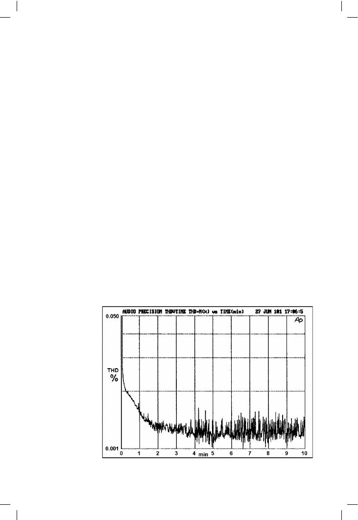
Figure 12.34 shows the THD plot taken over 10 minutes, starting from cold
and initiating some serious power dissipation at t = 0. The crossover
distortion drops at once; Figure 12.1 shows that driver dissipation is not
much affected by output level, so this must be due to the output device
junctions heating up and increasing Vq. There is then a slower reduction
until the THS reading stabilises at about 3 minutes.
The second amplifier structure examined is more complex. It is a triple-EF
design with drivers and output devices mounted on a large heatsink with
considerable thermal inertia. The pre-drivers are TO220 devices mounted
separately without heatsinks. It may seem perverse to mount the drivers on
365
Figure 12.34
Peak THD vs time
over 10 minutes

Audio Power Amplifier Design Handbook
the same heatsink as the outputs, because some of the time they are being
heated up rather than cooled down, which is exactly the opposite of what
is required to minimise Vbe changes. However, they need a heatsink of
some sort, and given the mechanical complications of providing a separate
thermally isolated heatsink just for the drivers, they usually end up on the
main heatsink. All that can be done (as in this case) is to put them in the
heatsink position that stays coolest in operation. Once more the bias sensor
transistor is not mounted on the main heatsink, but on the back of one of
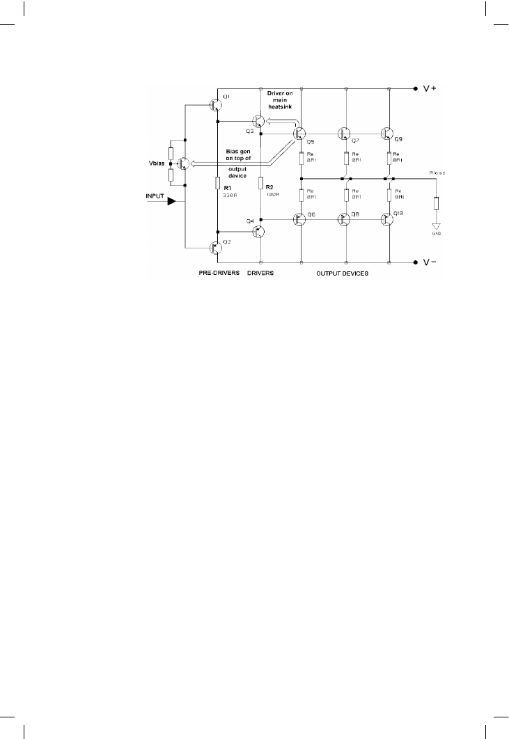
the output devices. See Figure 12.35 for the electrical circuit and thermal
coupling paths.
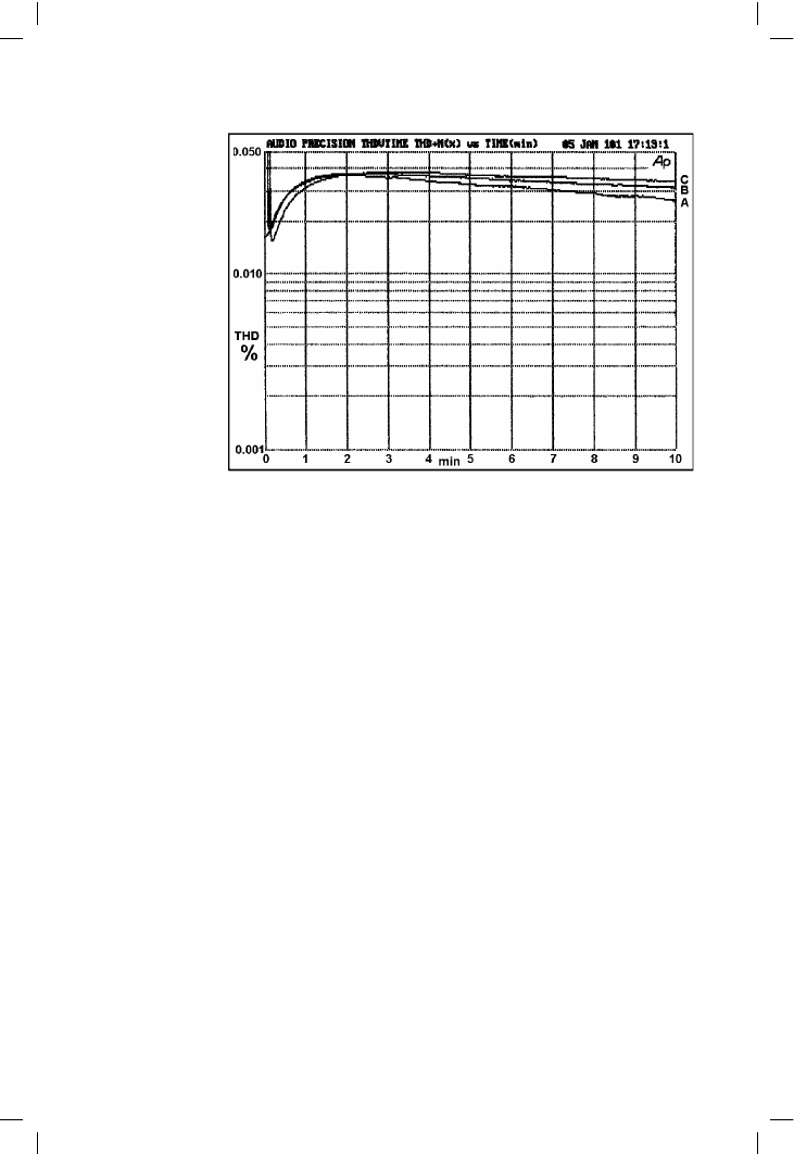
The results are quite different. Figure 12.36 shows at A the THD plot taken
over 10 minutes, again starting from cold and initiating dissipation at t = 0.
Initially THD falls rapidly, as before, as the output device junctions heat. It
then commences a slow rise over 2 minutes, indicative of falling bias, and
this represents the timelag in heating the sensor transistor. After this there is
a much slower drift downwards, at about the same rate as the main
heatsink is warming up. There are clearly at least three mechanisms
operating with very different time-constants. The final time-constant is very
long, and the immediate suspicion is that it must be related to the slow
warming of the main heatsink. Nothing else appears to be changing over
this sort of timescale. In fact this long-term increase in bias is caused by
cooling of the bias sensor compared with the output device it is mounted
on. This effect was theoretically predicted above, and it is pleasing to see
that it really exists, although it does nothing but further complicate the
quest for optimal Class-B operation. As the main heatsink gets hotter, the
heat losses from the sensor become more significant, and its temperature is
lower than it should be. Therefore the bias voltage generated is too high,
and this effect grows over time as the heatsink warms up.
366
Figure 12.35
Circuit and thermal
paths of the triple-EF
output stage

Thermal compensation and thermal dynamics
Knowledge of how the long-term drift occurs leads at once to a strategy for
reducing it. Adding thermal insulation to cover the sensor transistor, in the
form of a simple pad of plastic foam, gives plot B, with the long-term
variation reduced. Plot C reduces it still further by more elaborate
insulation; a rectangular block of foam with a cutout for the sensor
transistor. This is about as far as it is possible to go with sensor insulation;
the long-term variation is reduced to about 40% of what it was. While this
technique certainly appears to improve bias control, bear in mind that it is
being tested with a steady sinewave. Music is noted for not being at the
same level all the time, and its variations are much faster than the slow
effect we are examining. It is very doubtful if elaborate efforts to reduce
sensor cooling are worthwhile. I must admit this is the first time I have
applied thermal lagging to an amplifier output stage.
Early effect in output stages
There is another factor that affects the accuracy with which quiescent
conditions can be maintained. If you take a typical power amplifier and
power it from a variable-voltage transformer, you are very likely to find that
Vq varies with the mains voltage applied. This at first seems to indicate that
the apparently straightforward business of compensating the bias generator
for changes in standing current has fallen somewhat short of success (see
page 178). However, even if this appears to be correct, and the constant-
current source feeding the bias generator and VAS is made absolutely
stable, the quiescent conditions are still likely to vary. At first this seems
utterly mysterious, but the true reason is that the transistors in the output
367
Figure 12.36
Peak THD vs time
over 10 seconds

Audio Power Amplifier Design Handbook
stage are reacting directly to the change in their collector–emitter voltage
(Vce). As Vce increases, so does the Vq and the quiescent current. This is
called Early Effect. It is a narrowing of the base-collector region as Vce
increases, which will cause an increase in the collector current Ic even if
Vbe and Ib are held constant. In a practical EF output stage the result is a
significant variation in quiescent conditions when the supply voltage is
varied over a range such as ±10%.
Table 12.7 shows the effect as demonstrated by SPICE simulation, using
MJE340/50 for drivers and MJ15022/23 as output devices, with fixed bias
voltage of 2.550 V, which gave optimal crossover in this case. It is
immediately obvious that (as usual) things are more complicated than they
at first appear. The Vq increases with rail voltage, which matches reality.
However, the way in which this occurs is rather unexpected. The Vbe’s of
the drivers Q1 and Q2 reduce with increasing Vce as expected. However,
the output devices Q3 and Q4 show a Vbe that increases – but by a lesser
amount, so that after subtracting all the Vbe drops from the fixed bias
voltage the aggregate effect is that Vq, and hence quiescent current Iq, both
increase. Note that the various voltages have been summed as a check that
they really do add up to 2.550 V in each case.
Table 12.8 has the results of real Vbe measurements. These are not easy to
do, because any increase in Iq increases the heating in the various
transistors, which will cause their Vbe’s to drift. This happens to such an
extent that sensible measurements are impossible. The measurement
technique was therefore slightly altered. The amplifier was powered up on
the minimum rail voltage, with its Vq set to 1.0 mV only. This is far too low
for good linearity, but minimises heating while at the same time ensuring
that the output devices are actually conducting. The various voltages were
measured, the rail voltage increased by 5 V, and then the bias control
turned down as quickly as possible to get Vq back to 1.0 mV, and the
process is repeated. The results are inevitably less tidy as the real Vbe’s are
prone to wander around by a millivolt or so, but it is clear that in reality, as
in SPICE, most of the Early Effect is in the drivers, and there is a general
368
Table 12.7
SPICE Vbe
changes with
supply rail voltage
(MJE340/50 and
MJ15022/3). All
devices held at
25°C
±rail
V
Vq
mV
Q1 Vbe
mV
Q3 Vbe
mV
Q2 Vbe
mV
Q4 Vbe
mV
Sum
V
10
7.8
609
633
654
646
2.550
20
13
602
640
647
648
2.550
30
18
597
643
641
649
2.550
40
23
593
647
637
650
2.550
50
28
589
649
634
650
2.550

Thermal compensation and thermal dynamics
reduction in aggregate Vbe as rail voltage increases. The sum of Vbe’s is no
longer constant as Vq has been constrained to be constant instead.
It may seem at this point as if the whole business of quiescent control is just
too hopelessly complicated. Not so. The cure for the Early Effect problem
is to overcompensate for standing current changes, by making the value of
resistor R3 above larger than usual. The best and probably the only
practical way to find the right value is the empirical method. Wind the HT
up and down on the prototype design and adjust the value of R3 until the
Vq change is at a minimum. (Unfortunately this interacts with the bias
setting, so there is a bit of twiddling to do – however, for a given design you
only need to find the optimal value for R3 once.) This assumes that the
supply-rail rejection of the VAS current source is predictable and stable;
with the circuits normally used this seems to be the case, but some further
study in this area is required.
References
1. Sato et al Amplifier Transient Crossover Distortion Resulting from
Temperature Change of Output Power Transistors AES Preprint. AES
Preprint 1896 for 72nd Convention, Oct. 1982.
2. Brown, I Opto-Bias Basis for Better Power Amps Electronics World, Feb.
1992, p. 107.
3. Carslaw and Jaeger Conduction of Heat in Solids Oxford Univ. Press
1959, ISBN 0-19-853368-3.
4. Murphy, D Axisymmetric Model of a Moving-Coil Loudspeaker Journ.
AES, Sept. 1993, p. 679.
5. Motorola, Toulouse Private communication.
6. Evans, J Audio Amplifier Bias Current Letters Electronics & Wireless
World, Jan. 1991, p. 53.
7. Chen, C-T Analog & Digital Control System Design Saunders-HBJ 1993,
p. 346.
8. Harriot, P Process Control McGraw-Hill 1964, pp. 100–102.
9. Liptak, B, ed. Instrument Engineer’s Handbook-Process Control Butter-
worth-Heinemann 1995, p. 66.
369
Table 12.8
Real Vbe changes
with supply rail
voltage (2SC4382,
2SA1668 drivers
and 2SC2922,
2SA1216 output)
±rail
V
Vq
mV
Q1 Vbe
mV
Q3 Vbe
mV
Q2 Vbe
mV
Q4 Vbe
mV
Sum
V
40
1.0
554
568
541
537
2.201
45
1.0
544
556
533
542
2.176
50
1.0
534
563
538
536
2.172
55
1.0
533
549
538
540
2.161
60
1.0
527
552
536
535
2.151
65
1.0
525
540
536
539
2.141
70
1.0
517
539
537
539
2.133