ВУЗ: Казахская Национальная Академия Искусств им. Т. Жургенова
Категория: Учебное пособие
Дисциплина: Не указана
Добавлен: 03.02.2019
Просмотров: 17357
Скачиваний: 18

2
History, architecture and
negative feedback
A brief history of amplifiers
A full and detailed account of semiconductor amplifier design since its
beginnings would be a book in itself – and a most fascinating volume it
would be. This is not that book, but I still feel obliged to give a very brief
account of how amplifier design has evolved in the last three or four
decades.
Valve amplifiers, working in push-pull Class-A or AB1, and perforce
transformer-coupled to the load, were dominant until the early 1960s,
when truly dependable transistors could be made at a reasonable price.
Designs using germanium devices appeared first, but suffered severely from
the vulnerability of germanium to even moderately high temperatures; the
term thermal runaway was born. At first all silicon power transistors were
NPN, and for a time most transistor amplifiers relied on input and output
transformers for push-pull operation of the power output stage. These
transformers were as always heavy, bulky, expensive, and non-linear, and
added insult to injury as their LF and HF phase-shifts severely limited the
amount of negative feedback that could be safely applied.
The advent of the transformerless Lin configuration
[1]
, with what became
known as a quasi-complementary output stage, disposed of a good many
problems. Since modestly capable PNP driver transistors were available,
the power output devices could both be NPN, and still work in push-pull.
It was realised that a transformer was not required for impedance matching
between power transistors and 8 ! loudspeakers.
Proper complementary power devices appeared in the late 1960s, and full
complementary output stages soon proved to give less distortion than their
quasi-complementary predecessors. At about the same time DC-coupled
30

History, architecture and negative feedback
amplifiers began to take over from capacitor-coupled designs, as the
transistor differential pair became a more familiar circuit element.
A much fuller and generally excellent history of power amplifier
technology is given in Sweeney and Mantz
[2]
.
Amplifier architectures
This grandiose title simply refers to the large-scale structure of the amplifier;
i.e. the block diagram of the circuit one level below that representing it as
a single white block labelled Power Amplifier. Almost all solid-state
amplifiers have a three-stage architecture as described below, though they
vary in the detail of each stage.
The three-stage architecture
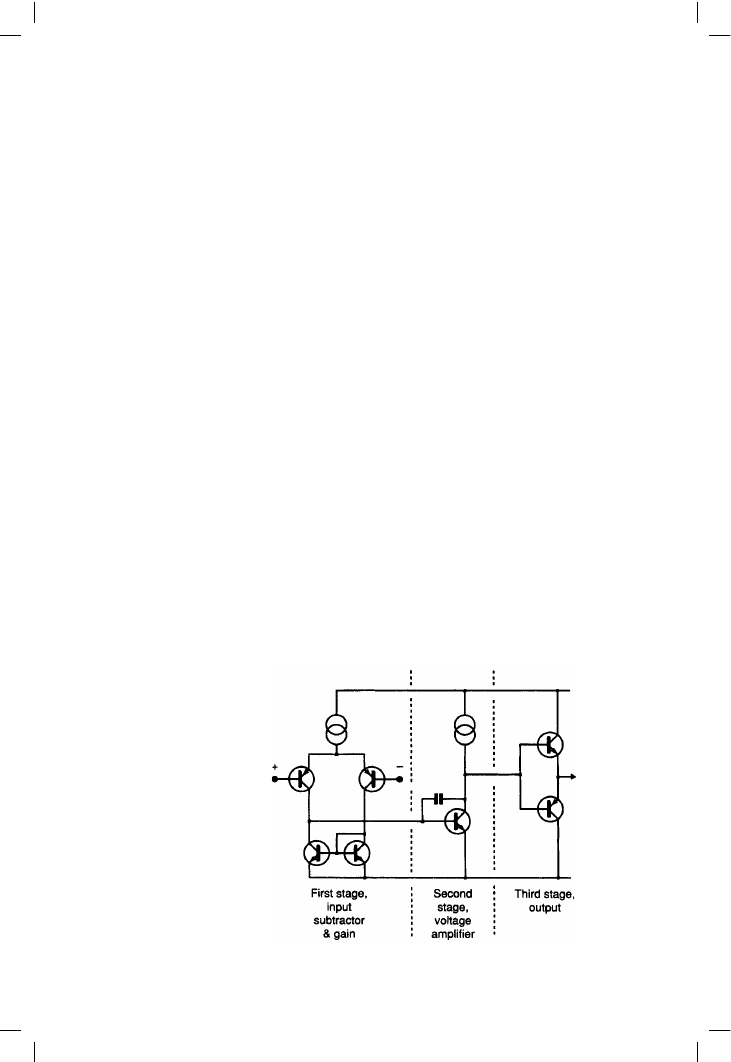
The vast majority of audio amplifiers use the conventional architecture,
shown in Figure 2.1. There are three stages, the first being a trans-
conductance stage (differential voltage in, current out) the second a
transimpedance stage (current in, voltage out) and the third a unity-voltage-
gain output stage. The second stage clearly has to provide all the voltage gain
and I have therefore called it the voltage-amplifier stage or VAS. Other
authors have called it the pre-driver stage but I prefer to reserve this term for
the first transistors in output triples. This three-stage architecture has several
advantages, not least being that it is easy to arrange things so that interaction
between stages is negligible. For example, there is very little signal voltage
at the input to the second stage, due to its current-input (virtual-earth) nature,
and therefore very little on the first stage output; this minimises Miller phase-
shift and possible Early effect in the input devices.
31
Figure 2.1
The three-stage
amplifier structure.
There is a
transconductance
stage, a
transadmittance stage
(the VAS) and a unity-
gain buffer output
stage

Audio Power Amplifier Design Handbook
Similarly, the compensation capacitor reduces the second stage output
impedance, so that the non-linear loading on it due to the input impedance
of the third stage generates less distortion than might be expected. The
conventional three-stage structure, familiar though it may be, holds several
elegant mechanisms such as this. They will be fully revealed in later
chapters. Since the amount of linearising global NFB available depends
upon amplifier open-loop gain, how the stages contribute to this is of great
interest. The three-stage architecture always has a unity-gain output stage –
unless you really want to make life difficult for yourself – and so the total
forward gain is simply the product of the transconductance of the input
stage and the transimpedance of the VAS, the latter being determined solely
by the Miller capacitor Cdom, except at very low frequencies. Typically, the
closed-loop gain will be between +20 and +30 dB. The NFB factor at
20 kHz will be 25 to 40 dB, increasing at 6 dB per octave with falling
frequency until it reaches the dominant pole frequency P1, when it flattens
out. What matters for the control of distortion is the amount of negative
feedback (NFB) available, rather than the open-loop bandwidth, to which
it has no direct relationship. In my Electronics World Class-B design, the
input stage gm is about 9 ma/V, and Cdom is 100 pF, giving an NFB factor
of 31 dB at 20 kHz. In other designs I have used as little as 26 dB (at 20 kHz)
with good results.
Compensating a three-stage amplifier is relatively simple; since the pole at
the VAS is already dominant, it can be easily increased to lower the HF
negative-feedback factor to a safe level. The local NFB working on the VAS
through Cdom has an extremely valuable linearising effect.
The conventional three-stage structure represents at least 99% of the solid-
state amplifiers built, and I make no apology for devoting much of this book
to its behaviour. I doubt if I have exhausted its subtleties.
The two-stage amplifier architecture
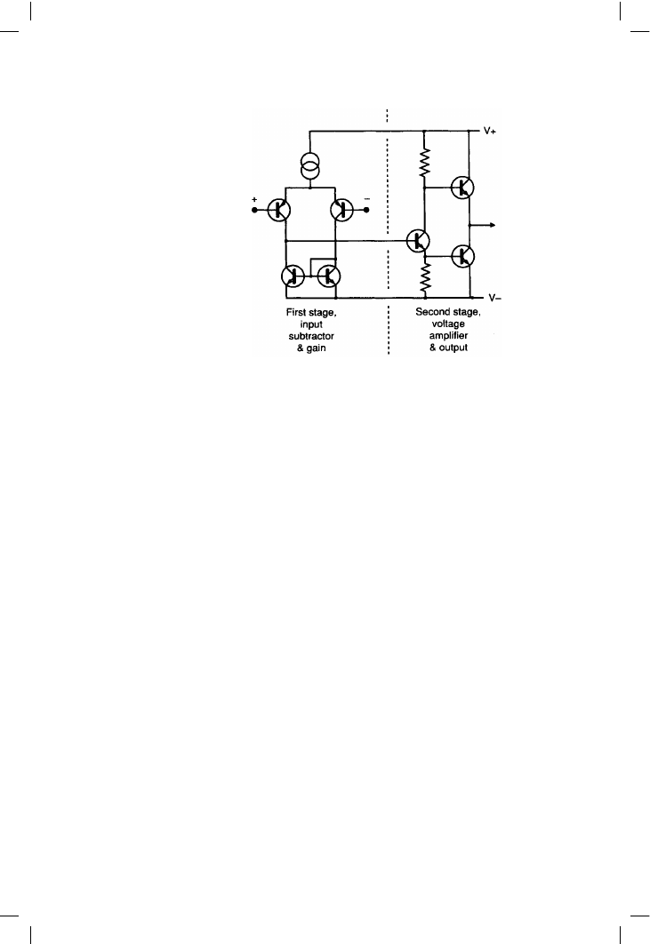
In contrast, the architecture in Figure 2.2 is a two-stage amplifier, the first
stage being once more a transconductance stage, though now without a
guaranteed low impedance to accept its output current. The second stage
combines VAS and output stage in one block; it is inherent in this scheme
that the VAS must double as a phase splitter as well as a generator of raw
gain. There are then two quite dissimilar signal paths to the output, and it
is not at all clear that trying to break this block down further will assist a
linearity analysis. The use of a phase-splitting stage harks back to valve
amplifiers, where it was inescapable as a complementary valve technology
has so far eluded us.
Paradoxically, a two-stage amplifier is likely to be more complex in its gain
structure than a three-stage. The forward gain depends on the input stage
gm, the input stage collector load (because the input stage can no longer be
32

History, architecture and negative feedback
assumed to be feeding a virtual earth) and the gain of the output stage,
which will be found to vary in a most unsettling manner with bias and
loading. Choosing the compensation is also more complex for a two-stage
amplifier, as the VAS/phase-splitter has a significant signal voltage on its
input and so the usual pole-splitting mechanism that enhances Nyquist
stability by increasing the pole frequency associated with the input stage
collector will no longer work so well. (I have used the term Nyquist
stability, or Nyquist oscillation throughout this book to denote oscillation
due to the accumulation of phase-shift in a global NFB loop, as opposed to
local parasitics, etc.)
The LF feedback factor is likely to be about 6 dB less with a 4 ! load, due
to lower gain in the output stage. However, this variation is much reduced
above the dominant pole frequency, as there is then increasing local NFB
acting in the output stage.
Two-stage amplifiers are not popular; I can quote only two examples,
Randi
[3]
and Harris
[4]
. The two-stage amplifier offers little or no reduction
in parts cost, is harder to design and in my experience invariably gives a
poor distortion performance.
Power amplifier classes
For a long time the only amplifier classes relevant to high-quality audio
were Class-A and Class-AB. This is because valves were the only active
devices, and Class-B valve amplifiers generated so much distortion that
they were barely acceptable even for Public Address purposes. All
amplifiers with pretensions to high fidelity operated in push-pull Class-A.
33
Figure 2.2
The two-stage amplifier
structure. A voltage-
amplifier output follows
the same
transconductance input
stage

Audio Power Amplifier Design Handbook
Solid-state gives much more freedom of design; all of the amplifier classes
below have been commercially exploited. Unfortunately, there will only be
space to deal in detail in this book with A, AB, and B, though this certainly
covers the vast majority of solid-state amplifiers. Plentiful references are
given so that the intrigued can pursue matters further.
Class-A
In a Class-A amplifier current flows continuously in all the output devices,
which enables the non-linearities of turning them on and off to be avoided.
They come in two rather different kinds, although this is rarely explicitly
stated, which work in very different ways. The first kind is simply a Class-B
stage (i.e. two emitter-followers working back-to-back) with the bias
voltage increased so that sufficient current flows for neither device to cut off
under normal loading. The great advantage of this approach is that it
cannot abruptly run out of output current; if the load impedance becomes
lower than specified then the amplifier simply takes brief excursions into
Class AB, hopefully with a modest increase in distortion and no seriously
audible distress.
The other kind could be called the controlled-current-source (VCIS) type,
which is in essence a single emitter-follower with an active emitter load for
adequate current-sinking. If this latter element runs out of current capability
it makes the output stage clip much as if it had run out of output voltage.
This kind of output stage demands a very clear idea of how low an
impedance it will be asked to drive before design begins.
Valve textbooks will be found to contain enigmatic references to classes of
operation called AB1 and AB2; in the former grid current did not flow for
any part of the cycle, but in the latter it did. This distinction was important
because the flow of output-valve grid current in AB2 made the design of the
previous stage much more difficult.
AB1 or AB2 has no relevance to semiconductors, for in BJT’s base current
always flows when a device is conducting, while in power FET’s gate
current never does, apart from charging and discharging internal
capacitances.
Class-AB
This is not really a separate class of its own, but a combination of A and B.
If an amplifier is biased into Class-B, and then the bias further increased, it
will enter AB. For outputs below a certain level both output devices
conduct, and operation is Class-A. At higher levels, one device will be
turned completely off as the other provides more current, and the distortion
jumps upward at this point as AB action begins. Each device will conduct
between 50% and 100% of the time, depending on the degree of excess
bias and the output level.
34