ВУЗ: Казахская Национальная Академия Искусств им. Т. Жургенова
Категория: Учебное пособие
Дисциплина: Не указана
Добавлен: 03.02.2019
Просмотров: 17378
Скачиваний: 18

Audio Power Amplifier Design Handbook
increasing from 0.10% to 0.16%; for 10% imbalance this deteriorates badly
to 0.55%. Unsurprisingly, imbalance in the other direction (Ic1>Ic2) gives
similar results.
Imbalance defined as deviation of Ic (per device) from that value which
gives equal currents in the pair.
This explains the complex distortion changes that accompany the
apparently simple experiment of altering the value of R2
[3]
. We might
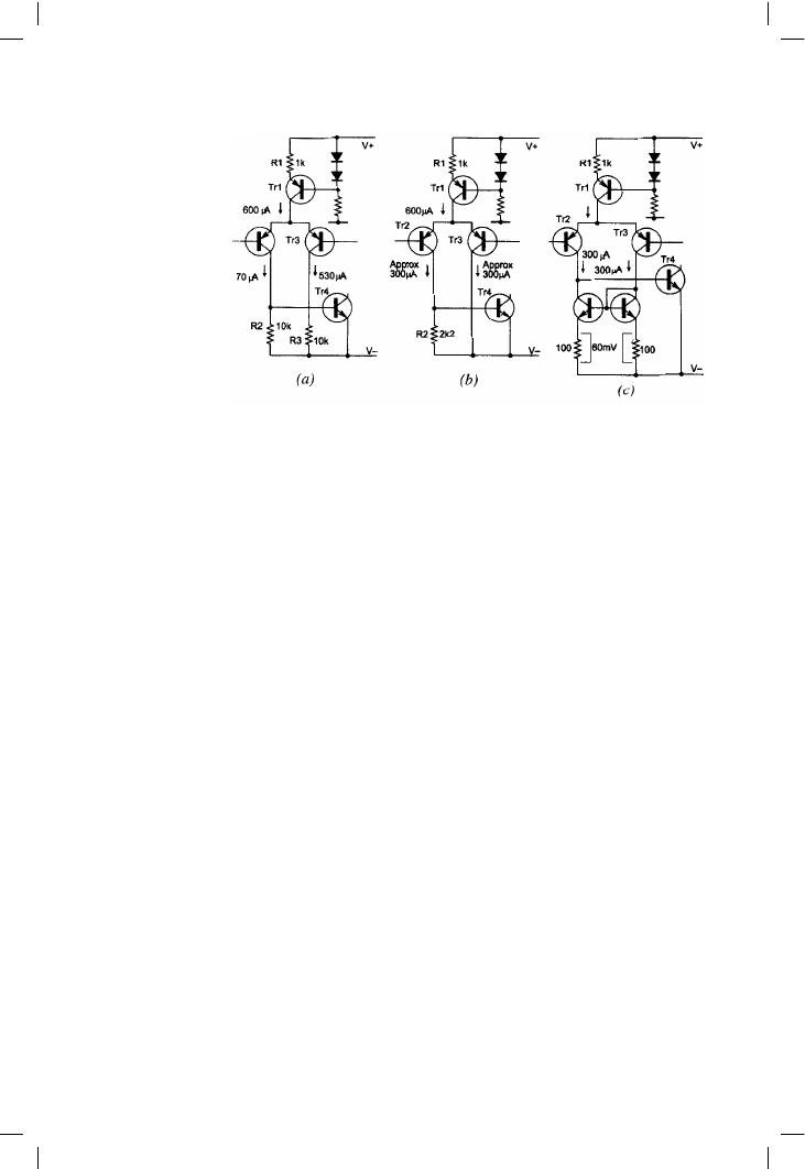
design an input stage like Figure 4.7a, where R1 has been selected as 1k
by uninspired guesswork and R2 made highish at 10k in a plausible but
misguided attempt to maximise o/l gain by minimising loading on Q1
collector. R3 is also 10k to give the stage a notional balance, though
unhappily this is a visual rather than electrical balance. The asymmetry is
shown in the resulting collector currents; the design generates a lot of
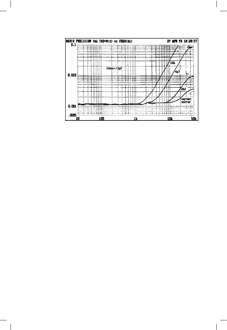
avoidable second harmonic distortion, displayed in the 10k curve of
Figure 4.8.
Recognising the crucial importance of DC balance, the circuit can be
rethought as Figure 4.7b. If the collector currents are to be roughly equal,
then R2 must be about 2
× R1, as both have about 0.6 V across them. The
dramatic effect of this simple change is shown in the 2k2 curve of Figure
4.8; the improvement is accentuated as the o/l gain has also increased by
some 7 dB, though this has only a minor effect on the closed-loop linearity
compared with the improved balance of the input pair. R3 has been excised
as it contributes very little to input stage balance.
The joy of current-mirrors
Although the input pair can be approximately balanced by the correct
values for R1 and R2, we remain at the mercy of several circuit tolerances.
Figure 4.6 shows that balance is critical, needing an accuracy of 1% or
80
Figure 4.7
Improvements to the
input pair. a Poorly
designed version.
b Better; partial
balance by correct
choice of R2. c Best;
near-perfect Ic
balance enforced by
mirror

The small signal stages
better for optimal linearity and hence low distortion at HF, where the input
pair works hardest. The standard current-mirror configuration in Figure
4.7c forces the two collector currents very close to equality, giving correct
cancellation of the second harmonic; the great improvement that results is
seen in the current-mirror curve of Figure 4.8. There is also less DC offset
due to unequal base-currents flowing through input and feedback
resistances; I often find that a power-amplifier improvement gives at
least two separate benefits. This simple mirror has well-known residual
base-current errors but they are not large enough to affect the distortion
performance.
The hyperbolic-tangent law also holds for the mirrored pair
[4]
, though the
output current swing is twice as great for the same input voltage as the
resistor-loaded version. This doubled output is given at the same distortion
as for the unmirrored version, as linearity depends on the input voltage,
which has not changed. Alternatively, we can halve the input and get the
same output, which with a properly balanced pair generating third
harmonic only will give one-quarter the distortion. A pleasing result.
The input mirror is made from discrete transistors, regretfully foregoing the
Vbe-matching available to IC designers, and it needs its own emitter-
degeneration for good current-matching. A voltage-drop across the current-
mirror emitter-resistors in the range 30–60 mV will be enough to make the
effect of Vbe tolerances on distortion negligible; if degeneration is omitted
then there is significant variation in HF distortion performance with
different specimens of the same transistor type.
Putting a current-mirror in a well-balanced input stage increases the total
o/l gain by at least 6 dB, and by up to 15 dB if the stage was previously
poorly balanced; this needs to be taken into account in setting the
81
Figure 4.8
Distortion of model
amplifier:
a Unbalanced with
R2 = 10k. b Partially
balanced with R =
2k2. c Accurately
balanced by current-
mirror

Audio Power Amplifier Design Handbook
compensation. Another happy consequence is that the slew-rate is roughly
doubled, as the input stage can now source and sink current into Cdom
without wasting it in a collector load. If Cdom is 100 pF, the slew-rate of
Figure 4.7b is about 2.8 V/µsec up and down, while 4.7c gives 5.6 V/µsec.
The unbalanced pair at 4.7a displays further vices by giving 0.7 V/µsec
positive-going and 5 V/µsec negative-going.
Improving input-stage linearity
Even if the input pair has a current-mirror, we may still feel that the HF
distortion needs further reduction; after all, once it emerges from the noise
floor it octuples with each doubling of frequency, and so it is well worth
postponing the evil day until as far as possible up the frequency range. The
input pair shown has a conventional value of tail-current. We have seen
that the stage transconductance increases with Ic, and so it is possible to
increase the gm by increasing the tail-current, and then return it to its
previous value (otherwise Cdom would have to be increased proportion-
ately to maintain stability margins) by applying local NFB in the form of
emitter-degeneration resistors. This ruse powerfully improves input linear-
ity, despite its rather unsettling flavour of something-for-nothing. The
transistor non-linearity can here be regarded as an internal non-linear
emitter resistance re, and what we have done is to reduce the value of this
(by increasing Ic) and replaced the missing part of it with a linear external
resistor Re.
For a single device, the value of re can be approximated by:
re = 25/Ic ohms (for Ic in mA)
Equation 4.3
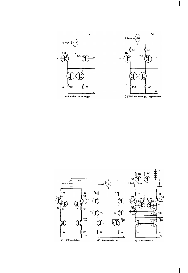
Our original stage at Figure 4.9a has a per-device Ic of 600 µA, giving a
differential (i.e. mirrored) gm of 23 mA/V and re = 41.6 !. The improved
version at Figure 4.9b has Ic = 1.35 mA and so re = 18.6 !; therefore
emitter degeneration resistors of 22 ! are required to reduce the gm back
to its original value, as 18.6 + 22 = 41.6 !. The distortion measured by the
circuit of Figure 4.4 for a –40 dBu input voltage is reduced from 0.32% to
0.032%, which is an extremely valuable linearisation, and will translate
into a distortion reduction at HF of about 5 times for a complete amplifier;
for reasons that will emerge later the full advantage is rarely gained. The
distortion remains a visually pure third-harmonic, so long as the input pair
remains balanced. Clearly this sort of thing can only be pushed so far, as the
reciprocal-law reduction of re is limited by practical values of tail current.
A name for this technique seems to be lacking; constant-gm degeneration
is descriptive but rather a mouthful.
The standing current is roughly doubled so we have also gained a higher
slew-rate; it has theoretically increased from 10 V/µsec to 20 V/µsec, and
once again we get two benefits for the price of one inexpensive
modification.
82

The small signal stages
Radical methods of improving input linearity
If we are seeking still better linearity, various techniques exist. Whenever it
is needful to increase the linearity of a circuit, it is often a good approach
to increase the local feedback factor, because if this operates in a tight local
NFB loop there is often little effect on the overall global-loop stability. A
reliable method is to replace the input transistors with complementary-
feedback (CFP or Sziklai) pairs, as shown in the stage of Figure 4.10a. If an
isolated input stage is measured using the test circuit of Figure 4.4, the
constant-gm degenerated version shown in Figure 4.9b yields 0.35% third-
harmonic distortion for a –30 dBu input voltage, while the CFP version
83
Figure 4.9
Input pairs before and
after constant-gm
degeneration, showing
how to double stage
current while keeping
transconductance
constant; distortion is
reduced by about ten
times
Figure 4.10
Some enhanced
differential pairs: a The
Complementary
Feedback Pair. b The
Cross-quad. c The
Cascomp

Audio Power Amplifier Design Handbook
gives 0.045%. (Note that the input level here is 10 dB up on the previous
example, to get well clear of the noise floor.) When this stage is put to work
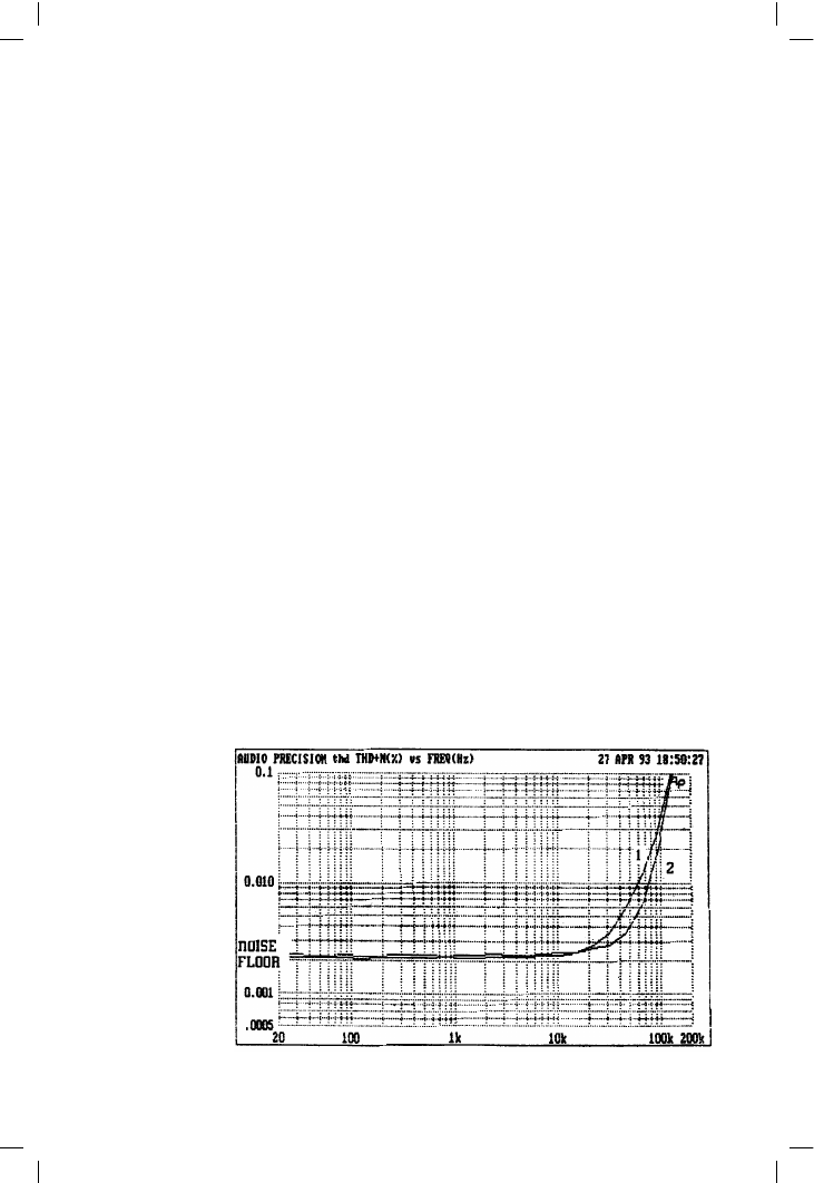
in a model amplifier, the third-harmonic distortion at a given frequency is
roughly halved, assuming all other distortion sources have been appro-
priately minimised. However, given the high-slope of input-stage distortion,
this only extends the low-distortion regime up in frequency by less than an
octave. See Figure 4.11.
A compromise is required in the CFP circuit on the value of Rc, which sets
the proportion of the standing current that goes through the NPN and PNP
devices on each side of the stage. A higher value of Rc gives better linearity,
but more noise, due to the lower Ic in the NPN devices that are the inputs
of the input stage, as it were, causing them to match less well the relatively
low source resistances. 2k2 is a good compromise.
Several other elaborations of the basic input pair are possible, although
almost unknown in the audio community. We are lucky in power-amp
design as we can tolerate a restricted input common-mode range that
would be unusable in an op-amp, giving the designer great scope.
Complexity in itself is not a serious disadvantage as the small-signal stages
of the typical amplifier are of almost negligible cost compared with mains
transformers, heatsinks, etc.
Two established methods to produce a linear input transconductance stage
(referred to in op-amp literature simply as a transconductor) are the cross-
quad
[5]
and the cascomp
[6]
configurations. The cross-quad (Figure 4.10b)
gives a useful reduction in input distortion when operated in isolation but
is hard to incorporate in a practical amplifier because it relies on very low
source-resistances to tame the negative conductances inherent in its
operation. The cross-quad works by imposing the input voltage to each half
84
Figure 4.11
Whole-amplifier THD
with normal and CFP
input stages; input
stage distortion only
shows above noise
floor at 20 kHz, so
improvement occurs
above this frequency.
The noise floor
appears high as the
measurement
bandwidth is 500 kHz