ВУЗ: Казахская Национальная Академия Искусств им. Т. Жургенова
Категория: Учебное пособие
Дисциплина: Не указана
Добавлен: 03.02.2019
Просмотров: 17374
Скачиваний: 18

Audio Power Amplifier Design Handbook
Using model amplifiers
Distortions 1 and 2 can dominate amplifier performance and need to be
studied without the manifold complications introduced by a Class-B output
stage. This can be done by reducing the circuit to a model amplifier that
consists of the small-signal stages alone, with a very linear Class-A emitter-
follower attached to the output to allow driving the feedback network; here
small-signal refers to current rather than voltage, as the model amplifier
should be capable of giving a full power-amp voltage swing, given
sufficiently high rail voltages. From Figure 3.2 it is clear that this will allow
study of Distortions 1 and 2 in isolation, and using this approach it will
prove relatively easy to design a small-signal amplifier with negligible
distortion across the audio band, and this is the only sure foundation on
which to build a good power amplifier.
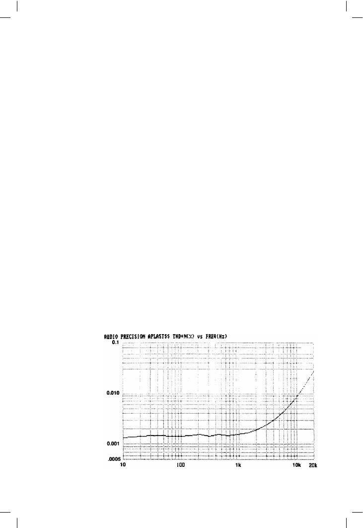
A typical plot combining Distortions 1 and 2 from a model amp is shown
in Figure 3.6, where it can be seen that the distortion rises with an
accelerating slope, as the initial rise at 6 dB/octave from the VAS is
contributed to and then dominated by the 12 dB/octave rise in distortion
from an unbalanced input stage.
The model can be powered from a regulated current-limited PSU to cut
down the number of variables, and a standard output level chosen for
comparison of different amplifier configurations; the rails and output level
used for the results in this work were +/–15 V and +16 dBu. The rail
voltages can be made comfortably lower than the average amplifier HT rail,
so that radical bits of circuitry can be tried out without the creation of a
silicon cemetery around your feet. It must be remembered that some
phenomena such as input-pair distortion depend on absolute output level,
70
Figure 3.6
The distortion from a
model amplifier,
produced by the input
pair and the Voltage-
Amplifier Stage – note
increasing slope as
input pair distortion
begins to add to VAS
distortion

The general principles of power amplifiers
rather than the proportion of the rail voltage used in the output swing, and
will be increased by a mathematically predictable amount when the real
voltage swings are used.
The use of such model amplifiers requires some caution, and gives no
insight into BJT output stages, whose behaviour is heavily influenced by the
sloth and low current gain of the power devices. As a general rule, it should
be possible to replace the small-signal output with a real output stage and
get a stable and workable power amplifier; if not, then the model is
probably dangerously unrealistic.
The concept of the Blameless amplifier
Here I introduce the concept of what I have chosen to call a Blameless
audio power amplifier. This is an amplifier designed so that all the easily-
defeated distortion mechanisms have been rendered negligible. (Note that
the word Blameless has been carefully chosen to not imply Perfection, but
merely the avoidance of known errors.) Such an amplifier gives about
0.0005% THD at 1 kHz and approximately 0.003% at 10 kHz when driving
8 !. This is much less THD than a Class-B amplifier is normally expected
to produce, but the performance is repeatable, predictable, and definitely
does not require large global feedback factors.
Distortion 1 cannot be totally eradicated, but its onset can be pushed
well above 20 kHz by the use of local feedback. Distortion 2 (VAS
distortion) can be similarly suppressed by cascoding or beta-enhance-
ment, and Distortions 4 to 7 can be made negligible by simple
topological methods. All these measures will be detailed later. This leaves
Distortion 3, which includes the intractable Class-B problems, i.e.
crossover distortion (Distortion 3b) and HF switch-off difficulties (Distor-
tion 3c). Minimising 3b requires a Blameless amplifier to use a BJT output
rather than FETs.
A Blameless Class-B amplifier essentially shows crossover distortion only,
so long as the load is no heavier than 8 !; this distortion increases with
frequency as the amount of global NFB falls. At 4 ! loading an extra
distortion mechanism (3a) generates significant third harmonic.
The importance of the Blameless concept is that it represents the best
distortion performance obtainable from straightforward Class-B. This
performance is stable and repeatable, and varies little with transistor type as
it is not sensitive to variable quantities such as beta.
Blamelessness is a condition that can be defined with precision, and is
therefore a standard other amplifiers can be judged against. A Blameless
design represents a stable point of departure for more radical designs, such
as the Trimodal concept in Chapter 9. This may be the most important use
of the idea.
71

Audio Power Amplifier Design Handbook
References
1. Oliver Distortion In Complementary-Pair Class-B Amplifiers Hewlett-
Packard Journal Feb 1971, p. 11.
2. Feucht Handbook of Analog Circuit Design Academic Press 1990,
p. 256 (Pole-splitting).
3. Cherry, E A New Distortion Mechanism in Class-B Amplifiers Journ.
Audio Eng. Soc. May 1981, p. 327.
4. Ball, G Distorting Power Supplies Electronics World+WW, Dec 1990,
p. 1084.
72

4
The small signal stages
‘A beginning is the time for taking the most delicate care that the
balances are correct.’ Frank Herbert, Dune.
The role of the input stage
The input stage of an amplifier performs the critical duty of subtracting the
feedback signal from the input, to generate the error signal that drives the
output. It is almost invariably a differential transconductance stage; a
voltage-difference input results in a current output that is essentially
insensitive to the voltage at the output port. Its design is also frequently
neglected, as it is assumed that the signals involved must be small, and that
its linearity can therefore be taken lightly compared with that of the VAS or
the output stage. This is quite wrong, for a misconceived or even mildly
wayward input stage can easily dominate the HF distortion performance.
The input transconductance is one of the two parameters setting HF open-
loop (o/l) gain, and therefore has a powerful influence on stability and
transient behaviour as well as distortion. Ideally the designer should set out
with some notion of how much o/l gain at 20 kHz will be safe when driving
worst-case reactive loads (this information should be easier to gather now
there is a way to measure o/l gain directly) and from this a suitable
combination of input transconductance and dominant-pole Miller capaci-
tance can be chosen.
Many of the performance graphs shown here are taken from a model
(small-signal stages only) amplifier with a Class-A emitter-follower output,
at +16 dBu on +/–15 V rails; however, since the output from the input pair
is in current form, the rail voltage in itself has no significant effect on the
linearity of the input stage; it is the current swing at its output that is the
crucial factor.
73

Audio Power Amplifier Design Handbook
Distortion from the input stage
The motivation for using a differential pair as the input stage of an amplifier
is usually its low DC offset. Apart from its inherently lower offset due to the
cancellation of the Vbe voltages, it has the important added advantage that
its standing current does not have to flow through the feedback network.
However a second powerful reason, which seems less well-known, is that
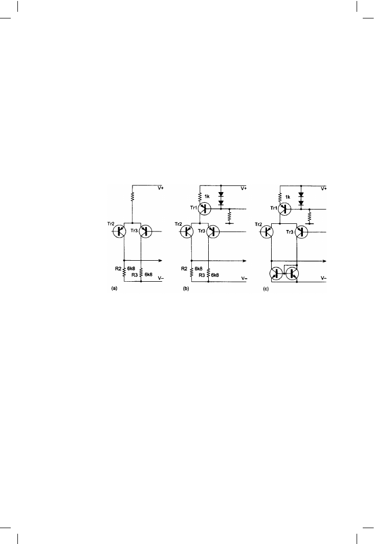
linearity is far superior to single-transistor input stages. Figure 4.1 shows
three versions, in increasing order of sophistication. The resistor-tail version
at 1a has poor CMRR and PSRR and is generally a false economy of the
shabbiest kind; it will not be further considered here. The mirrored version
at 1c has the best balance, as well as twice the transconductance of 1b.
At first sight, the input stage should generate a minimal proportion of the
overall distortion because the voltage signals it handles are very small,
appearing as they do upstream of the VAS that provides almost all the
voltage gain. However, above the first pole frequency P1, the current
required to drive Cdom dominates the proceedings, and this remorselessly
doubles with each octave, thus:
i
pk
= w
× C
dom
× V
pk
Equation 4.1
where W = 2
× pi × freq
For example the current required at 100 W (8 !) and 20 kHz, with a 100 pF
Cdom is 0.5 mA peak, which may be a large proportion of the input
standing current, and so the linearity of transconductance for large current
excursions will be of the first importance if we want low distortion at high
frequencies.
Curve A in Figure 4.2 shows the distortion plot for a model amplifier (at
+16 dBu output) designed so the distortion from all other sources is
negligible compared with that from the carefully balanced input stage; with
a small-signal class A stage this reduces to making sure that the VAS is
74
Figure 4.1
Three versions of an
input pair. a Simple
tail resistor. b Tail
current-source. c With
collector current-mirror
to give inherently
good lc balance