ВУЗ: Казахская Национальная Академия Искусств им. Т. Жургенова
Категория: Учебное пособие
Дисциплина: Не указана
Добавлен: 03.02.2019
Просмотров: 17376
Скачиваний: 18

The small signal stages
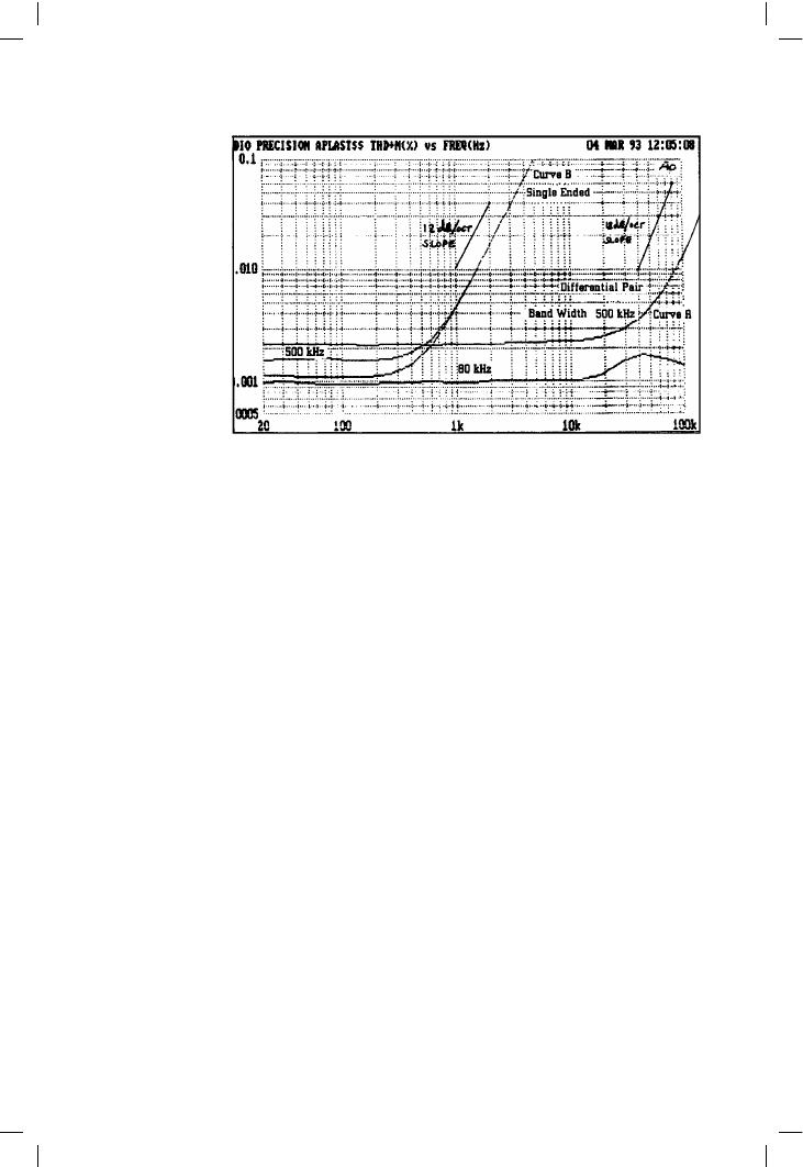
properly linearised. Plots are shown for both 80 kHz and 500 kHz
measurement bandwidths, in an attempt to show both HF behaviour and
the vanishingly low LF distortion. It can be seen that the distortion is below
the noise floor until 10 kHz, when it emerges and heaves upwards at a
precipitous 18 dB/octave. This rapid increase is due to the input stage signal
current doubling with every octave, to feed Cdom; this means that the
associated third harmonic distortion will quadruple with every octave
increase. Simultaneously the overall NFB available to linearise this
distortion is falling at 6 dB/octave since we are almost certainly above the
dominant-pole frequency P1, and so the combined effect is an octuple or
18 dB/octave rise. If the VAS or the output stage were generating distortion
this would be rising at only 6 dB/octave, and so would look quite different
on the plot.
This non-linearity, which depends on the rate-of-change of the output
voltage, is the nearest thing that exists to the late unlamented TID (Transient
Intermodulation Distortion), an acronym that now seems to be falling out of
fashion. SID (Slew-Induced-Distortion) is a better description of the effect,
but implies that slew-limiting is responsible, which is not the case.
If the input pair is not accurately balanced, then the situation is more
complex. Second as well as third harmonic distortion is now generated,
and by the same reasoning this has a slope nearer to 12 dB/octave; this vital
point is examined more closely below.
BJTs vs FETs for the input stage
At every stage in the design of an amplifier, it is perhaps wise to consider
whether BJTs or FETs are the best devices for the job. I may as well say
75
Figure 4.2
Distortion performance
of model amplifier-
differential pair at A
compared with
singleton input at B.
The singleton
generates copious
second-harmonic
distortion

Audio Power Amplifier Design Handbook
at once that the predictable Vbe/Ic relationship and much higher
transconductance of the bipolar transistor make it, in my opinion, the best
choice for all three stages of a generic power amplifier. To quickly
summarise the position:
Advantages of the FET input stage
There is no base current with FETs, so this is eliminated as a source of DC
offset errors. However, it is wise to bear in mind that FET gate leakage
currents increase very rapidly with temperature, and under some circum-
stances may need to be allowed for.
Disadvantages of FET input stage
1 The undegenerated transconductance is low compared with BJTs. There
is much less scope for linearising the input stage by adding degeneration
in the form of source resistors, and so an FET input stage will be very non-
linear compared with a BJT version degenerated to give the same low
transconductance,
2 the Vgs offset spreads will be high. Having examined many different
amplifier designs, it seems that in practice it is essential to use dual FETs,
which are relatively very expensive and not always easy to obtain. Even
then, the Vgs mismatch will probably be greater than Vbe mismatch in
a pair of cheap discrete BJTs; for example the 2N5912 N-channel dual
FET has a specified maximum Vgs mismatch of 15 mV. In contrast the
Vbe mismatches of BJTs, especially those taken from the same batch
(which is the norm in production) will be much lower, at about 2–3 mV,
and usually negligible compared with DC offset caused by unbalanced
base currents,
3 the noise performance will be inferior if the amplifier is being driven
from a low-impedance source, say 5 k! or less. This is almost always the
case.
Singleton input stage versus differential pair
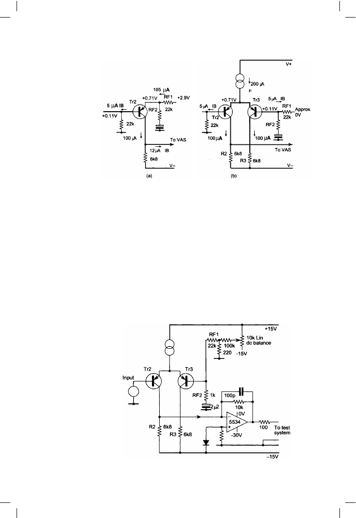
Using a single input transistor (Figure 4.3a) may seem attractive, where the
amplifier is capacitor-coupled or has a separate DC servo; it at least
promises strict economy. However, the snag is that this singleton
configuration has no way to cancel the second-harmonics generated in
copious quantities by its strongly-curved exponential Vin/lout character-
istic
[1]
. The result is shown in Figure 4.2 curve-B, where the distortion is
much higher, though rising at the slower rate of 12 dB/octave.
The input stage distortion in isolation
Examining the slope of the distortion plot for the whole amplifier
is instructive, but for serious research we need to measure input-stage
76

The small signal stages
non-linearity in isolation. This can be done with the test circuit of Figure
4.4. The op-amp uses shunt feedback to generate an appropriate AC virtual-
earth at the input-pair output. Note that this current-to-voltage conversion
op-amp requires a third –30 V rail to allow the i/p pair collectors to work
at a realistic DC voltage – i.e. about one diode’s-worth above the –15 V rail.
Rf can be scaled as convenient, to stop op-amp clipping, without the input
stage knowing anything has changed. The DC balance of the pair can be
manipulated by VR1, and it is instructive to see the THD residual diminish
as balance is approached, until at its minimum amplitude it is almost pure
third harmonic.
77
Figure 4.3
Singleton and
differential pair input
stages, showing
typical DC
conditions. The large
DC offset of the
singleton is mainly
due to all the stage
current flowing
through the feedback
resistor RF1
Figure 4.4
Test circuit for
examining input stage
distortion in isolation.
The shunt-feedback
op-amp is biased to
provide the right DC
conditions for TR2

Audio Power Amplifier Design Handbook
The differential pair has the great advantage that its transfer characteristic is
mathematically highly predictable
[2]
. The output current is related to the
differential input voltage Vin by:
I
out
= I
e
.tanh(–V
in
/2V
t
)
Equation 4.2
(where Vt is the usual thermal voltage of about 26 mV at 25°C, and le the
tail current).
Two vital facts derived from this equation are that the transconductance
(gm) is maximal at Vin = 0, when the two collector currents are equal, and
that the value of this maximum is proportional to the tail current le. Device
beta does not figure in the equation, and the performance of the input pair
is not significantly affected by transistor type.
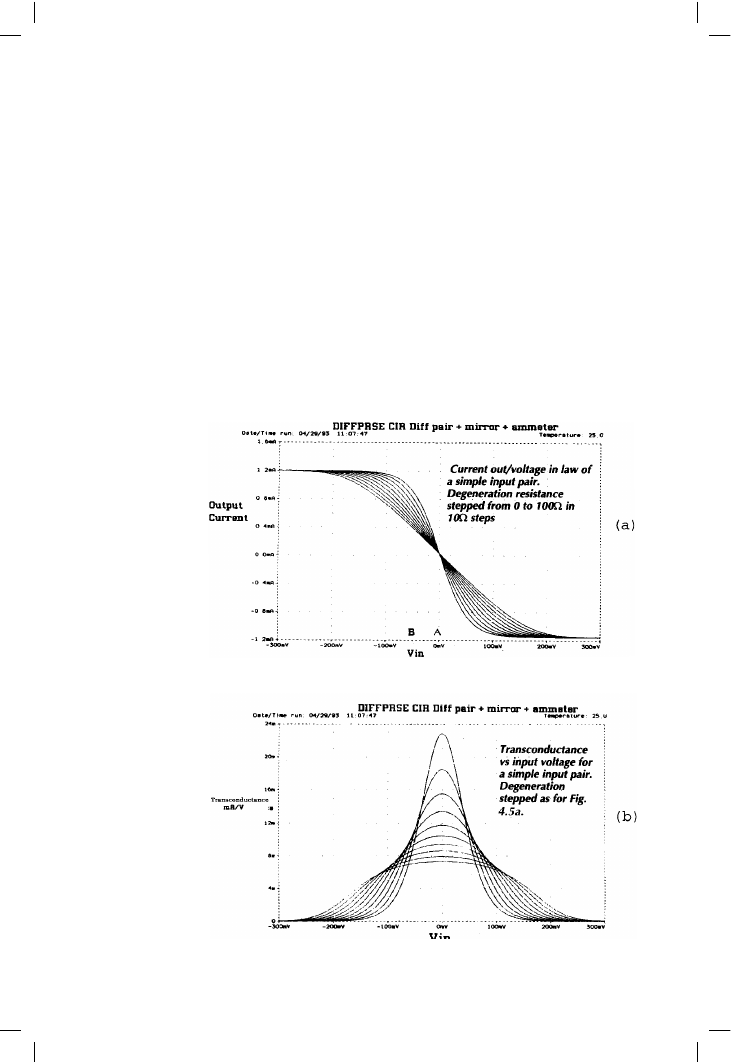
Figure 4.5a shows the linearising effect of local feedback or degeneration
on the voltage-in/current-out law; Figure 4.5b plots transconductance
78
Figure 4.5
Effect of
degeneration on
input pair V/I law,
showing how
transconductance is
sacrificed in favour
of linearity. (SPICE
simulation)

The small signal stages
against input voltage and shows clearly how the peak transconductance
value is reduced, but the curve made flatter and linear over a wider
operating range. Simply adding emitter degeneration markedly improves
the linearity of the input stage, but the noise performance is slightly
worsened, and of course the overall amplifier feedback factor has been
reduced, for as previously shown, the vitally-important HF closed-loop
gain is determined solely by the input transconductance and the value of
the dominant-pole capacitor.
Input stage balance
Exact DC balance of the input differential pair is essential in power
amplifiers. It still seems almost unknown that minor deviations from equal
Ic in the pair seriously upset the second-harmonic cancellation, by moving
the operating point from A in Figure 4.5a to B. The average slope of the
characteristic is greatest at A, so imbalance also reduces the open-loop gain
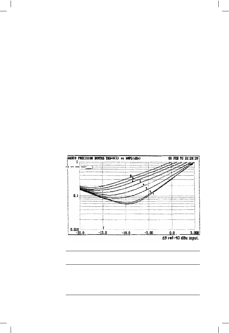
if serious enough. The effect of small amounts of imbalance is shown in
Figure 4.6 and Table 4.1; for an input of –45 dBu a collector-current
imbalance of only 2% gives a startling worsening of linearity, with THD
79
Figure 4.6
Effect of collector-
current imbalance on
an isolated input pair;
the second harmonic
rises well above the
level of the third if the
pair moves away from
balance by as little as
2%
Table 4.1
(Key to Figure 4.6) Curve No.
Ic Imbalance
Curve No.
Ic Imbalance
1
0%
5
5.4%
2
0.5%
6
6.9%
3
2.2%
7
8.5%
4
3.6%
8
10%