ВУЗ: Казахская Национальная Академия Искусств им. Т. Жургенова
Категория: Учебное пособие
Дисциплина: Не указана
Добавлен: 03.02.2019
Просмотров: 17385
Скачиваний: 18

Audio Power Amplifier Design Handbook
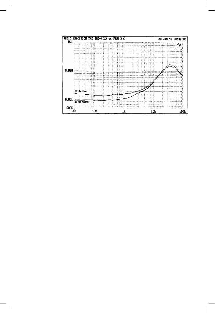
The use of a buffer is essential if a VAS cascode is to do some good. Figure
4.20 shows before/after distortion for a full-scale power amplifier with
cascode VAS driving 100 W into 8 !.
The balanced VAS
When we are exhorted to make the amplifier linear before adding negative
feedback one of the few specific recommendations made is usually the use
of a balanced VAS – sometimes combined with a double input stage
consisting of two differential amplifiers, one complementary to the other.
The latter seems to have little to recommend it, as you cannot balance a
stage that is already balanced, but a balanced (and, by implication, more
linear) VAS has its attractions. However, as explained above, the distortion
contribution from a properly-designed VAS is negligible under most
circumstances, and therefore there seems to be little to be gained.
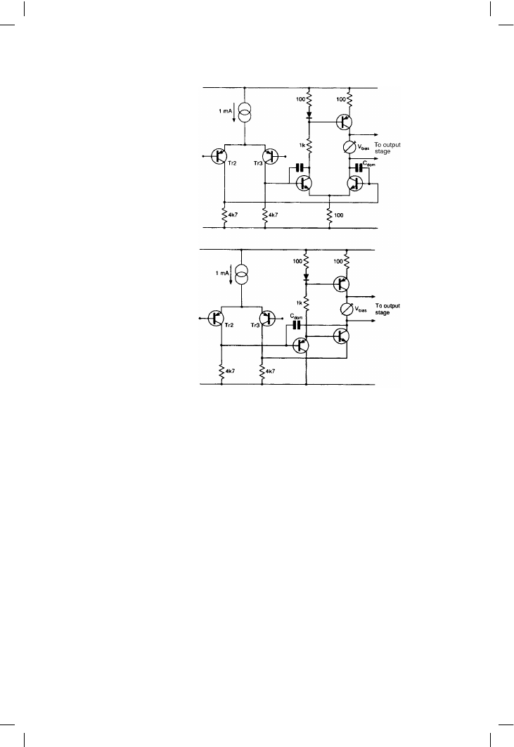
Two possible versions are shown in Figure 4.21; Type 1 gives approx-
imately 10 dB more o/l gain than the standard, but this naturally requires an
increase in Cdom if the same stability margins are to be maintained. In a
model amplifier, any improvement in linearity can be wholly explained by
this o/l gain increase, so this seems (not unexpectedly) an unpromising
approach. Also, as Linsley-Hood has pointed out
[12]
, the standing current
through the bias generator is ill-defined compared with the usual current-
source VAS; similarly the balance of the input pair is likely to be poor
compared with the current-mirror version. A further difficulty is that there
are now two signal paths from the input stage to the VAS output, and it is
difficult to ensure that these have the same bandwidth; if they do not then
a pole-zero doublet is generated in the open-loop gain characteristic that
will markedly increase settling-time after a transient. This seems likely to
apply to all balanced VAS configurations.
100
Figure 4.20
The beneficial effect
of using a VAS-buffer
in a full-scale Class-B
amplifier. Note that
the distortion needs to
be low already for the
benefit to be
significant

The small signal stages
Type 2 is attributed by Borbely to Lender
[13]
. Figure 4.21 shows one
version, with a quasi-balanced drive to the VAS transistor, via both base and
emitter. This configuration does not give good balance of the input pair, as
this is at the mercy of the tolerances of R2, R3, the Vbe of the VAS, and so
on. Borbely has advocated using two complementary versions of this,
giving Type 3, but it is not clear that this in any way overcomes the
objections above, and the increase in complexity is significant.
This can be only a brief examination of balanced VAS stages; many config-
urations are possible, and a comprehensive study of them all would be a
major undertaking. All seem to be open to the objection that the vital balance
of the input pair is not guaranteed, and that the current through the bias
generator is not well-defined. However one advantage would seem to be the
potential for sourcing and sinking large currents into Cdom, which might
improve the ultimate slew-rate and HF linearity of a very fast amplifier.
The VAS and manipulating open-loop bandwidth
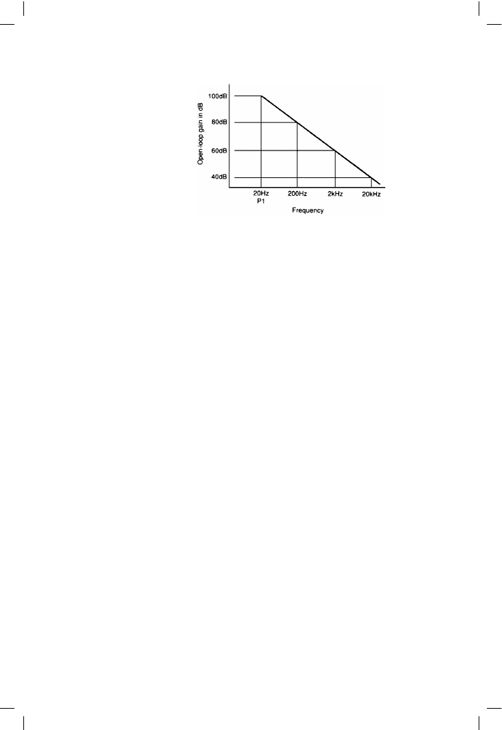
Acute marketing men will by now have realised that reducing the LF o/l
gain, leaving HF gain unchanged, must move the P1 frequency upwards, as
shown in Figure 4.22 Open-loop gain is held constant up to 2 kHz sounds
101
Figure 4.21
Two kinds of balanced
VAS: Type 1 gives
more open-loop gain,
but no better open-loop
linearity. Type 2 – the
circuit originated by
Lender

Audio Power Amplifier Design Handbook
so much better than the open-loop bandwidth is restricted to 20 Hz
although these two statements could describe near-identical amplifiers,
except that the first has plenty of open-loop gain at LF while the second has
even more than that. Both amplifiers have the same feedback factor at HF,
where the amount available has a direct effect on distortion performance,
and could easily have the same slew-rate. Nonetheless the second
amplifier somehow reads as sluggish and indolent, even when the truth of
the matter is known.
It therefore follows that reducing the LF o/l gain may be of interest to
commercial practitioners. Low values of open-loop gain also have their
place in the dogma of the subjectivist, and the best way to bring about this
state of affairs is worth examining, always bearing in mind that:
1 there is no engineering justification for it,
2 reducing the NFB factor will reveal more of the output stage distortion;
since in general NFB is the only weapon we have to deal with this,
blunting its edge seems ill-advised.
It is of course simple to reduce o/l gain by degenerating the input pair, but this
diminishes it at HF as well as LF. To alter it at LF only it is necessary to tackle
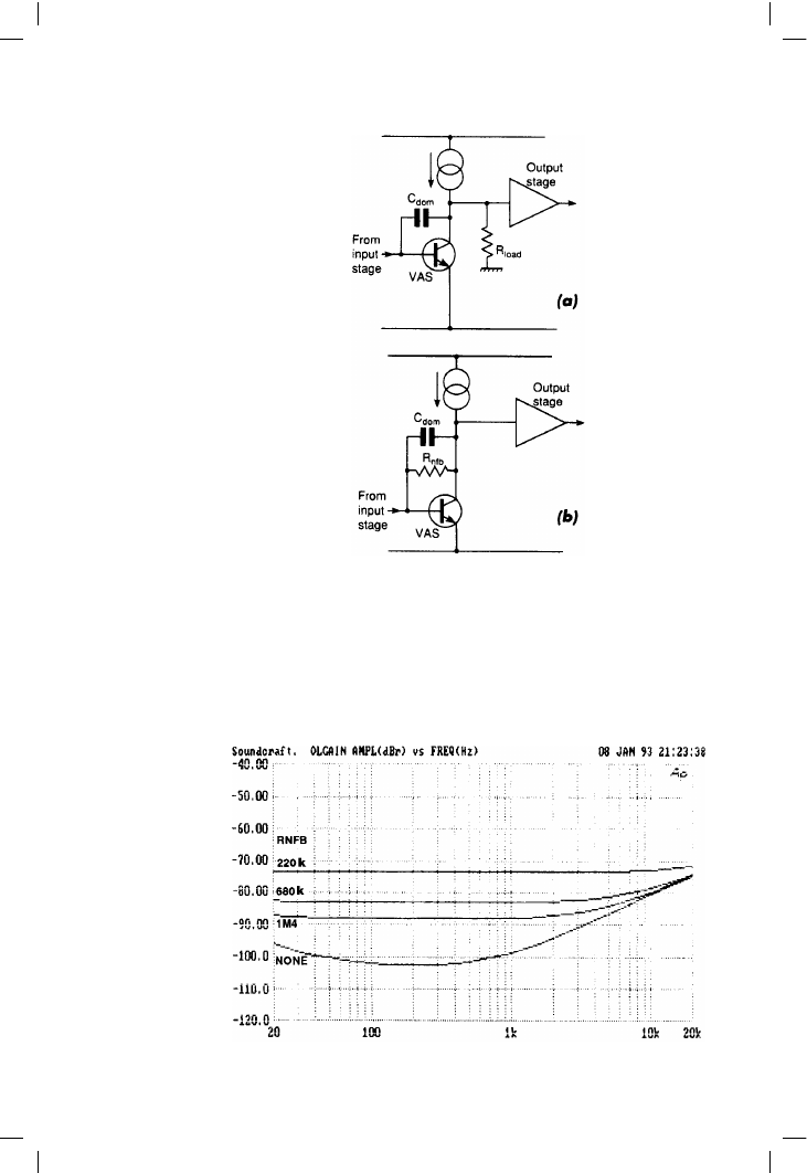
the VAS instead, and Figure 4.23 shows two ways to reduce its gain. Figure
4.23a reduces gain by reducing the value of the collector impedance, having
previously raised it with the use of a current-source collector load. This ain’t
no way to treat a gain stage; loading resistors low enough to have a
significant effect cause unwanted current variations in the VAS as well as
shunting its high collector impedance, and serious LF distortion appears.
While this sort of practice has been advocated in the past
[14]
, it seems to have
nothing to recommend it as it degrades VAS linearity at the same time as
syphoning off the feedback that would try to minimise the harm. Figure
4.23b also reduces overall o/l gain, but by adding a frequency-insensitive
component to the local shunt feedback around the VAS. The value of R
NFB
is
too high to load the collector significantly and therefore the full gain is
available for local feedback at LF, even before Cdom comes into action.
102
Figure 4.22
Showing how
dominant-pole
frequency P1 can be
altered by changing
the LF open-loop gain;
the gain at HF, which
determines Nyquist
stability and HF
distortion, is unaffected

The small signal stages
Figure 4.24 shows the effect on the open-loop gain of a model amplifier for
several values of R
NFB
; this plot is in the format described in Chapter 3, where
error-voltage is plotted rather than gain directly, and so the curve once more
appears upside down compared with the usual presentation. Note that the
dominant-pole frequency is increased from 800 Hz to above 20 kHz by
using a 220k value for R
NFB
; however the gain at higher frequencies is
103
Figure 4.23
Two ways to reduce
o/l gain:
a by simply loading
down the collector.
This is a cruel way
to treat a VAS;
current variations
cause extra
distortion
b local NFB with a
resistor in parallel
with Cdom. This
looks crude, but
actually works very
well
Figure 4.24
The result of VAS
gain-reduction by
local feedback; the
dominant pole
frequency is
increased from about
800 Hz to about
20 kHz, with high-
frequency gain hardly
affected

Audio Power Amplifier Design Handbook
unaffected and so is the stability. Although the amount of feedback available
at 1 kHz has been decreased by nearly 20 dB, the distortion at +16 dBu
output is only increased from less than 0.001 to 0.0013%; most of this
reading is due to noise.
In contrast, reducing the open-loop gain even by 10 dB by loading the VAS
collector to ground requires a load of 4k7, which under the same
conditions yields distortion of more than 0.01%.
Manipulating open-loop bandwidth
If the value of R
NFB
required falls below about 100K, then the standing
current flowing through it can become large enough to upset the amplifier
operating conditions (Figure 4.23b). This is revealed by a rise in distortion
above that expected from reducing the feedback factor, as the input stage
becomes unbalanced as a result of the global feedback straightening things
up. This effect can be simply prevented by putting a suitably large capacitor
in series with R
NFB
. A 2µ2 non-electrolytic works well, and does not cause
any strange response effects at low frequencies.
An unwelcome consequence of reducing the global negative feedback is
that power-supply rejection is impaired (see page 252). To prevent negative
supply-rail ripple reaching the output it is necessary to increase the filtering
of the V-rail that powers the input stage and the VAS. Since the voltage drop
in an RC filter so used detracts directly from the output voltage swing, there
are severe restrictions on the highest resistor value that can be tolerated.
The only direction left to go is increasing C, but this is also subject to
limitations as it must withstand the full supply voltage and rapidly becomes
a bulky and expensive item.
That describes the ‘brawn’ approach to improving PSRR. The ‘brains’
method is to use the input cascode compensation scheme described on
page 248. This solves the problem by eliminating the change of reference
at the VAS, and works extremely well with no compromise on HF stability.
No filtering at all is now required for the V-supply rail – it can feed the input
stage and VAS directly.
Conclusions
Hopefully the first half of this chapter has shown that input stage design is
not something to be taken lightly if low noise, low distortion, and low offset
are desired. A good design choice even for very high quality requirements
is a constant-gm-degenerated input pair with a degenerated current-mirror;
the extra cost of the mirror will be trivial.
The latter half of this chapter showed how the strenuous efforts of the input
circuitry can be best exploited by the voltage-amplifier stage following it. At
first it appears axiomatic that the stage providing all the voltage gain of an
104