ВУЗ: Казахская Национальная Академия Искусств им. Т. Жургенова
Категория: Учебное пособие
Дисциплина: Не указана
Добавлен: 03.02.2019
Просмотров: 17391
Скачиваний: 18

Audio Power Amplifier Design Handbook
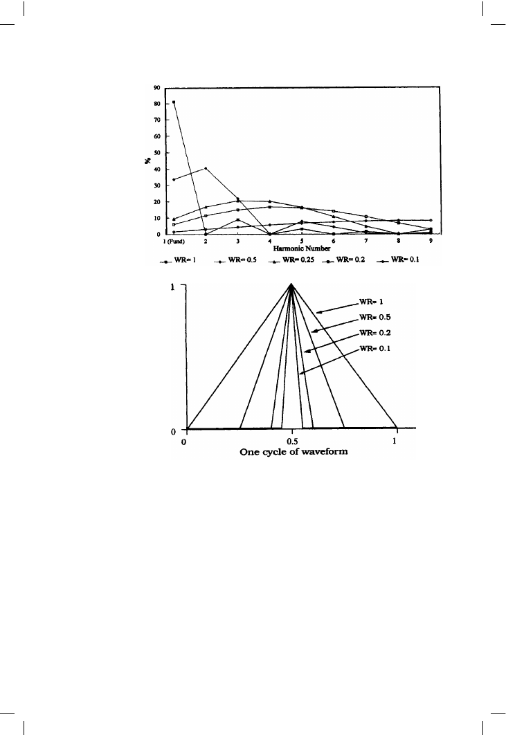
Figure 5.3 shows how the situation is made more like crossover or
switching distortion by squeezing the triangular error into the centre of the
cycle so that its value is zero elsewhere; now E is non-zero for only half the
cycle (denoted by WR = 0.5) and Figure 5.2 shows that the even harmonics
are no longer absent. As WR is further decreased, the energy is pushed into
higher-order harmonics, the amplitude of the lower falling.
The high harmonics have roughly equal amplitude, spectrum analysis (see
Figure 5.1, page 108) confirming that even in a Blameless amplifier driven
at 1 kHz, harmonics are freely generated from the seventh to the nineteenth
at an equal level to a dB or so. The nineteenth harmonic is only 10 dB
below the third.
Thus, in an amplifier with crossover distortion, the order of the harmonics
will decrease as signal amplitude reduces, and WR increases; their lower
110
Figure 5.2
The amplitude of each
harmonic changes with
WR; as the error
waveform gets
narrower, energy is
transferred to the
higher harmonics
Figure 5.3
Diagram of the error
waveform E for some
values of WR

The output stage I
frequencies allow them to be better corrected by the frequency-dependant
NFB. This effect seems to work against the commonly assumed rise of
percentage crossover distortion as level is reduced.
Comparing output stages
One of my aims in this book is to show how to isolate each source of
distortion so that it can be studied, (and hopefully reduced) with a
minimum of confusion and perplexity. When investigating output behav-
iour, it is perfectly practical to drive output stages open-loop, providing the
driving source-impedance is properly specified; this is difficult with a
conventional amplifier, as it means the output must be driven from a
frequency-dependant impedance simulating that at the VAS collector, with
some sort of feedback mechanism incorporated to keep the drive voltage
constant.
However, if the VAS is buffered from the output stage by some form of
emitter-follower, as advocated on page 99, it makes things much simpler, a
straightforward low-impedance source (e.g. 50 !) providing a good
approximation of conditions in a VAS-buffered closed-loop amplifier. The
VAS-buffer makes the system more designable by eliminating two variables
– the VAS collector impedance at LF, and the frequency at which it starts to
decrease due to local feedback through Cdom. This markedly simplifies the
study of output stage behaviour.
The large-signal linearity of various kinds of open-loop output stage with
typical values are shown in Figures 5.6–5.16. These diagrams were all
generated by SPICE simulation, and are plotted as incremental output gain
against output voltage, with the load resistance stepped from 16 to 2 !,
which I hope is the lowest impedance that feckless loudspeaker designers
will throw at us. They have come to be known as wingspread diagrams,
from their vaguely birdlike appearance. The power devices are MJ802 and
MJ4502, which are more complementary than many so-called pairs, and
minimise distracting large-signal asymmetry. The quiescent conditions are
in each case set to minimise the peak deviations of gain around the
crossover point for 8 ! loading; for the moment it is assumed that you can
set this accurately and keep it where you want it. The difficulties in actually
doing this will be examined later.
If we confine ourselves to the most straightforward output stages, there are
at least 16 distinct configurations, without including error-correcting
[3]
,
current-dumping
[4]
, or Blomley
[5]
types. These are:
Emitter-Follower
3 types
Figure 5.4
Complementary Feedback Pair
1 type
Figure 5.5
Quasi-Complementary
2 types
Figure 5.5
Output Triples
At least 7 types
Figure 5.6
Power FET
3 types
Chapter 11
111

Audio Power Amplifier Design Handbook
The emitter-follower output
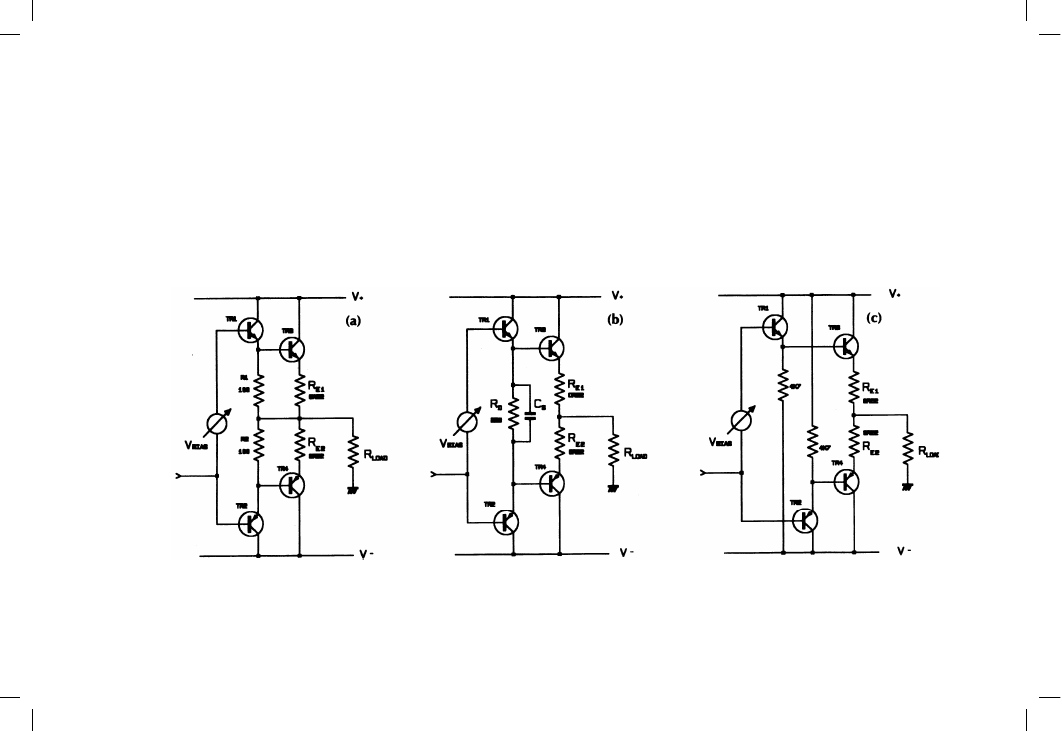
Three versions of the most common type of output stage are shown in
Figure 5.4; this is the double-emitter-follower, where the first follower acts
as driver to the second (output) device. I have deliberately called this an
Emitter-Follower (EF) rather than a Darlington configuration, as this latter
implies an integrated device that includes driver, output, and assorted
emitter resistors in one ill-conceived package. As for all the circuitry here,
the component values are representative of real practice. Important
attributes of this topology are:
1 the input is transferred to the output via two base-emitter junctions in
series, with no local feedback around the stage (apart from the very local
100% voltage feedback that makes an emitter-follower what it is),
2 there are two dissimilar base-emitter junctions between the bias voltage
and the emitter resistor Re, carrying different currents and at different
temperatures. The bias generator must attempt to compensate for both at
once, though it can only be thermally-coupled to one. The output
devices have substantial thermal inertia, and so any thermal compensa-
tion can only be a time-average of the preceding conditions. Figure 5.4a
shows the most prevalent version (Type I) which has its driver emitter
resistors connected to the output rail.
The Type II configuration in Figure 5.4b is at first sight merely a pointless
variation on Type I, but in fact it has a valuable extra property. The shared
driver emitter-resistor Rd, with no output-rail connection, allows the drivers
to reverse-bias the base-emitter junction of the output device being turned
off. Assume that the output voltage is heading downwards through the
crossover region; the current through Re1 has dropped to zero, but that
through Re2 is increasing, giving a voltage-drop across it, so TR4 base is
caused to go more negative to get the output to the right voltage. This
negative excursion is coupled to TR3 base through Rd, and with the values
shown can reverse bias it by up to –0.5 V, increasing to –1.6 V with a 4 !
load. The speed-up capacitor Cs markedly improves this action, preventing
the charge-suckout rate being limited by the resistance of Rd. While the
Type I circuit has a similar voltage drop across Re2, the connection of the
mid-point of R1, R2 to the output rail prevents this from reaching TR3 base;
instead TR1 base is reverse-biased as the output moves negative, and since
charge-storage in the drivers is usually not a problem, this does little good.
In Type II the drivers are never reverse-biased, though they do turn off. The
important issue of output turn-off and switching distortion is further
examined on page 153.
The Type III topology shown in Figure 5.4c maintains the drivers in Class-A
by connecting the driver Re’s to the opposite supply rail, rather than the
output rail. It is a common misconception
[6]
that Class-A drivers somehow
maintain better low-frequency control over the output devices, but I have
yet to locate any advantage myself. The driver dissipation is of course
112

113
Figure 5.4
Three types of
Emitter-Follower
output stages

Audio Power Amplifier Design Handbook
substantially increased, and nothing seems to be gained at LF as far as the
output transistors are concerned, for in both Type I and Type II the drivers
are still conducting at the moment the outputs turn off, and are back in
conduction before the outputs turn on, which would seem to be all that
matters. Type III is equally good as Type II at reverse-biasing the output
bases, and may give even cleaner HF turn-off as the carriers are being
swept from the bases by a higher resistance terminated in a higher voltage,
approximating constant-current drive; this remains to be determined by
experiment.
The large-signal linearity of these three versions is virtually identical – all
have the same feature of two base-emitter junctions in series between input
and load. The gain/output voltage plot is shown at Figure 5.7; with BJTs the
gain reduction with increasing loading is largely due to the Re’s. Note that
the crossover region appears as a relatively smooth wobble rather than a
jagged shape. Another major feature is the gain-droop at high output
voltages and low loads, and this gives us a clue that high collector currents
are the fundamental cause of this. A close-up of the crossover region gain
for 8 ! loading only is shown in Figure 5.8; note that no Vbias setting can
be found to give a constant or even monotonic gain; the double-dip and
central gain peak are characteristic of optimal adjustment. The region
extends over an output range of about +/–5 V, independent of load
resistance.
The CFP output
The other major type of bipolar complementary output is the Com-
plementary Feedback Pair (hereinafter CFP) sometimes called the Sziklai-
Pair, seen in Figure 5.5a. There seems to be only one popular configuration,
though versions with gain are possible. The drivers are now placed so that
they compare the output voltage with that at the input. Thus wrapping the
outputs in a local NFB loop promises better linearity than emitter-follower
versions with 100% feedback applied separately to driver and output
transistors.
The CFP topology is generally considered to show better thermal stability
than the EF, because the Vbe of the output devices is inside the local NFB
loop, and only the driver Vbe affects the quiescent conditions. The true
situation is rather more complex, and is explored in Chapter 12.
In the CFP output, like the EF, the drivers are conducting whenever the
outputs are, so special arrangements to keep them in Class-A seem
pointless. The CFP stage, like EF Type I, can only reverse-bias the driver
bases, and not the output bases, unless extra voltage rails outside the main
ones are provided.
The output gain plot is shown in Figure 5.9; Fourier analysis of this shows
that the CFP generates less than half the LSN of an emitter-follower stage.
114