ВУЗ: Казахская Национальная Академия Искусств им. Т. Жургенова
Категория: Учебное пособие
Дисциплина: Не указана
Добавлен: 03.02.2019
Просмотров: 17419
Скачиваний: 18

The output stage II
It is common for amplifiers to show a rise in distortion at the LF end, but
there is no reason why this should ever occur. Capacitor distortion is
usually the reason, but Distortion 5 (Rail Decoupling Distortion) can also
contribute. They can be distinguished because Distortion 5 typically rises
by only 6 dB/octave as frequency decreases, rather than 12–18 dB/
octave.
Amplifiers with AC-coupled outputs are now fairly rare, possibly because
distortion in the output capacitor is a major problem, occurring in the mid-
band as well as at LF. See page 42 for details.
Design example: a 50 W Class-B amplifier
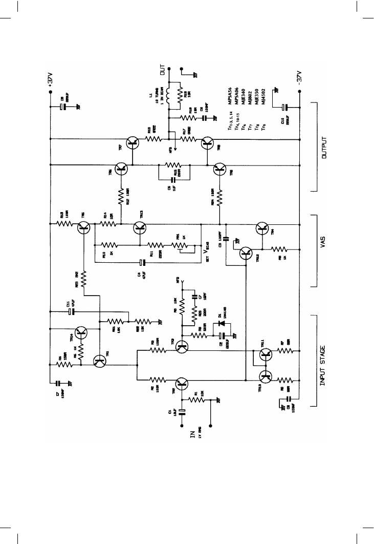
Figure 6.16 shows a design example of a Class-B amplifier, intended for
domestic hi-fi applications. Despite its relatively conventional appearance,
the circuit parameters selected give much better than a conventional
distortion performance; this is potentially a Blameless design, but only if
due care is given to wiring topology and physical layout will this be
achieved.
With the supply voltages and values shown it gives 50 W into 8 !, for
1 Vrms input. In earlier chapters I have used the word Blameless to describe
amplifiers in which all distortion mechanisms, except the apparently
unavoidable ones due to Class-B, have been rendered negligible. This
circuit has the potential to be Blameless, (as do we all) but achieving this
depends on care in cabling and layout. It does not aim to be a cookbook
project; for example, overcurrent and DC-offset protection are omitted.
In Chapter 11, output topologies are examined, and the conclusion drawn
that power-FETs were disappointingly expensive, inefficient, and non-
linear. Bipolars it is, therefore. The best BJT configurations were the
Emitter-Follower Type II, with least output switchoff distortion, and the
Complementary Feedback Pair (CFP), giving the best basic linearity.
The output configuration chosen is the Emitter-Follower Type II, which has
the advantage of reducing switchoff non-linearities (Distortion 3c) due to
the action of R15 in reverse-biasing the output base-emitter junctions as
they turn off. A possible disadvantage is that quiescent stability might be
worse than for the CFP output topology, as there is no local feedback loop
to servo out Vbe variations in the hot output devices. Domestic ambient
temperature changes will be small, so that adequate quiescent stability can
be attained by suitable heatsinking and thermal compensation.
A global NFB factor of 30 dB at 20 kHz was chosen, which should give
generous HF stability margins. The input stage (current-source TR1 and
differential pair TR2, 3) is heavily degenerated by R2, 3 to delay the onset
of third-harmonic Distortion 1, and to assist this the contribution of
transistor internal re variation is minimised by using the unusually high tail
175

Audio Power Amplifier Design Handbook
176
Figure
6.16
50
W
Class-B
amplifier
circuit
diagram.
Transistor
numbers
correspond
with
the
generic
amplifier
in
Chapter
3

The output stage II
current of 4 ma. TR11, 12 form a degenerated current-mirror that enforces
accurate balance of the TR2, 3 collector currents, preventing the generation
of second-harmonic distortion. Tail source TR1, 14 has a basic PSRR 10 dB
better than the usual two-diode version, though this is academic when C11
is fitted.
Input resistor R1 and feedback arm R8 are made equal and kept as low as
possible consistent with a reasonably high input impedance, so that base
current mismatch caused by beta variations will give a minimal DC offset;
this does not affect TR2–TR3 Vbe mismatches, which appear directly at the
output, but these are much smaller than the effects of lb. Even if TR2, 3 are
high voltage types with low beta, the output offset should be within
+/–50 mV, which should be quite adequate, and eliminates balance presets
and DC servos. A low value for R8 also gives a low value for R9, which
improves the noise performance.
The value of C2 shown (220 µF) gives an LF roll-off with R9 that is –3 dB at
1.4 Hz. The aim is not an unreasonably extended sub-bass response, but to
prevent an LF rise in distortion due to capacitor non-linearity; 100 µF
degraded the THD at 10 Hz from less than 0.0006% to 0.0011%, and I
judge this unacceptable aesthetically if not audibly. Band-limiting should
be done earlier, with non-electrolytic capacitors. Protection diode D1
prevents damage to C2 if the amplifier suffers a fault that makes it saturate
negatively; it looks unlikely but causes no measurable distortion
[5]
. C7
provides some stabilising phase-advance and limits the closed-loop
bandwidth; R20 prevents it upsetting TR3.
The VAS stage is enhanced by an emitter-follower inside the Miller-
compensation loop, so that the local NFB that linearises the VAS is
increased by augmenting total VAS beta, rather than by increasing the
collector impedance by cascoding. This extra local NFB effectively
eliminates Distortion 2 (VAS non-linearity). Further study has shown that
thus increasing VAS beta gives a much lower collector impedance than a
cascode stage, due to the greater local feedback, and so a VAS-buffer to
eliminate Distortion 4 (loading of VAS collector by the non-linear input
impedance of the output stage) appears unnecessary. Cdom is relatively
high at 100 pF, to swamp transistor internal capacitances and circuit strays,
and make the design predictable. The slew-rate calculates as 40 V/µsec.
The VAS collector-load is a standard current source, to avoid the
uncertainties of bootstrapping.
Since almost all the THD from a blameless amplifier is crossover, keeping
the quiescent conditions optimal is essential. Quiescent stability requires
the bias generator to cancel out the Vbe variations of four junctions in
series; those of two drivers and two output devices. Bias generator TR8 is
the standard Vbe-multiplier, modified to make its voltage more stable
against variations in the current through it. These occur because the biasing
of TR5 does not completely reject rail variations; its output current also
177

Audio Power Amplifier Design Handbook
drifts initially due to heating and changes in TR5 Vbe. Keeping Class-B
quiescent stable is hard enough at the best of times, and so it makes sense
to keep these extra factors out of the equation. The basic Vbe-multiplier has
an incremental resistance of about 20 !; in other words its voltage changes
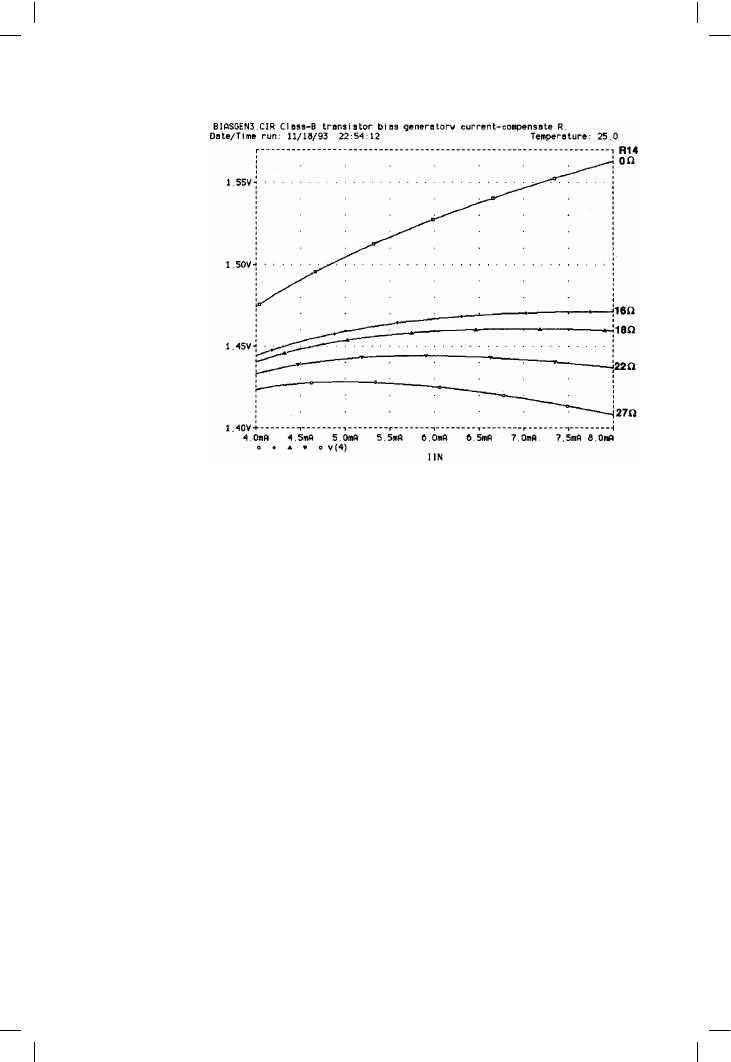
by 1 mV for a 50 µA drift in standing current. Adding R14 converts this to
a gently-peaking characteristic that can be made perfectly flat at one
chosen current; see Figure 6.17. Setting R14 to 22 ! makes the voltage
peak at 6 mA, and standing current now must deviate from this value by
more than 500 µA for a 1 mV bias change. The R14 value needs to be
altered if TR15 is run at a different current; for example, 16 ! makes the
voltage peak at 8 mA instead. If TO3 outputs are used the bias generator
should be in contact with the top or can of one of the output devices, rather
than the heatsink, as this is the fastest and least attenuated source for
thermal feedback.
The output stage is a standard double emitter-follower apart from the
connection of R15 between the driver emitters without connection to the
output rail. This gives quicker and cleaner switchoff of the outputs at high
frequencies; switchoff distortion may significantly degrade THD from
10 kHz upwards, dependent on transistor type. Speedup capacitor C4
noticeable improves the switchoff action. C6, R18 form the Zobel network,
(sometimes confusingly called a Boucherot cell) while L1, damped by R19,
isolates the amplifier from load capacitance.
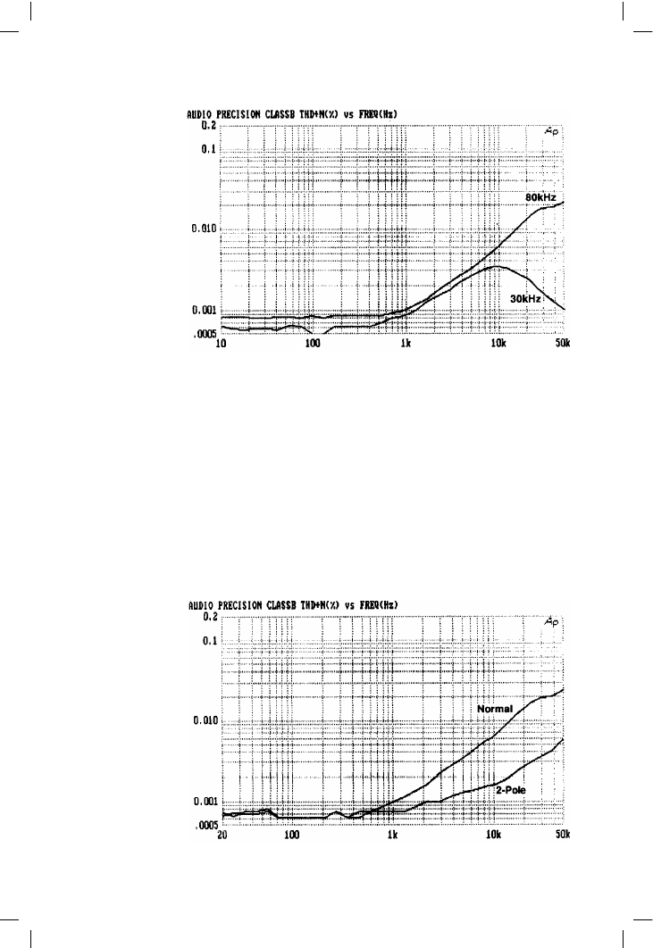
Figure 6.18 shows the 50 W/8 ! distortion performance; about 0.001% at
1 kHz, and 0.006% at 10 kHz. The measurement bandwidth makes a big
178
Figure 6.17
SPICE plot of the
voltage-peaking
behaviour of a current-
compensated bias
generator

The output stage II
difference to the appearance, because what little distortion is present is
crossover-derived, and so high-order. It rises at 6 dB/octave, at the rate the
feedback factor falls, and it is instructive to watch the crossover glitches
emerging from the noise, like Grendel from the marsh, as the test frequency
increases above 1 kHz. There is no precipitous THD rise in the ultrasonic
region.
The zigzags on the LF end of the plot are measurement artefacts, apparently
caused by the Audio Precision system trying to winkle out distortion from
visually pure white noise. Below 700 Hz the residual was pure noise with a
level equivalent to approx. 0.0006% (yes, three zeros) at 30 kHz bandwidth;
the actual THD here must be microscopic. This performance can only be
179
Figure 6.18
Class-B amplifier: THD
performance at
50 W/8 !;
measurement
bandwidths 30 kHz
and 80 kHz
Figure 6.19
The dramatic THD
improvement obtained
by converting the
Class-B amplifier to
2-pole compensation