ВУЗ: Казахская Национальная Академия Искусств им. Т. Жургенова
Категория: Учебное пособие
Дисциплина: Не указана
Добавлен: 03.02.2019
Просмотров: 17422
Скачиваний: 18

Compensation, slew-rate, and stability
while the VAS collector-load sources it, and likewise the input stage must
source it while the VAS sinks it, there are four possible ways in which slew-
rate may be limited by inadequate current capacity; if the input stage is
properly designed then the usual limiting factor is VAS current-sourcing. In
this example a peak current of less than 0.5 ma should be easy to deal with,
and the maximum frequency for unslewed output will be comfortably
above 20 kHz.
Lag compensation
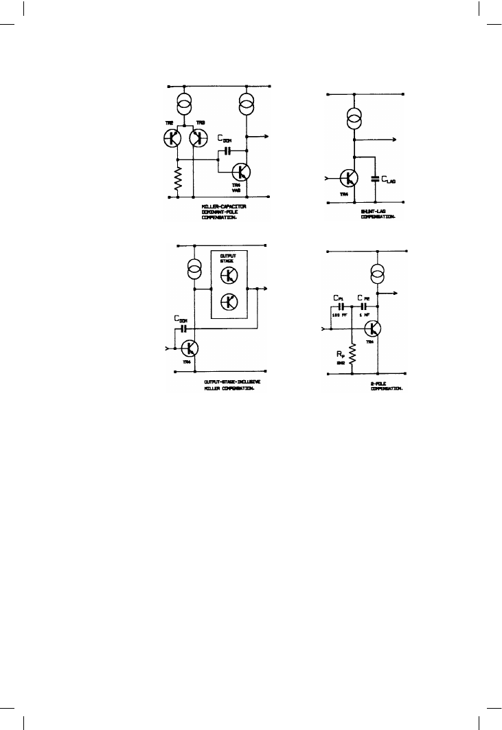
Figure 7.1b shows a much less satisfactory method of compensation – the
addition of capacitance to ground from the VAS collector. This is usually
called shunt or lag compensation, and as Peter Baxandall
[2]
aptly put it,
‘The technique is in all respects sub-optimal.’ We have already seen on
page 101 that loading the VAS collector resistively to ground is a very poor
option for reducing LF open-loop gain, and a similar argument shows that
capacitative loading to ground for compensation purposes is an even worse
185
Figure 7.1
(a) The traditional
Miller method of
making a dominant
pole. (b) Shunt
compensation shows a
much less satisfactory
method – the addition
of capacitance to
ground from the VAS
collector. (c) Inclusive
Miller compensation.
(d) Two-pole
compensation
(a)
(b)
(c)
(d)

Audio Power Amplifier Design Handbook
idea. To reduce open-loop gain at 20 kHz to 50 dB as before, the shunt
capacitor C
lag
must be 43.6 nF, which is a whole different order of things
from 125 pF. The current in and out of C
lag
at 20 V rms, 20 kHz, is 155 mA
peak, which is going to require some serious electronics to provide it. This
important result is yielded by simple calculation, confirmed by Spice
simulation. The input stage no longer constrains the slew-rate limits, which
now depend entirely on the VAS.
A VAS working under these conditions will have poor linearity. The lc
variations in the VAS, caused by the heavy extra loading, produce more
distortion and there is no local NFB through a Miller capacitor to correct it.
To make matters worse, the dominant pole P1 will probably need to be set
to a lower frequency than for the Miller case, to maintain the same stability
margins, as there is now no pole-splitting action to increase the frequency
of the pole at the input-stage collector. Hence C
lag
may have to be even
larger than 43 nF, requiring even higher peak currents.
Takahashi
[3]
has produced a fascinating paper on this approach, showing
one way of generating the enormous compensation currents required for
good slew-rates. The only thing missing is an explanation of why shunt
compensation was chosen in the first place.
Including the output stage: inclusive Miller compensation
Miller-capacitor compensation elegantly solves several problems at once,
and the decision to adopt it is simple. However the question of whether to
include the output stage in the Miller feedback loop is less easy. Such
inclusion (see Figure 7.1c) presents the alluring possibility that local
feedback could linearise both the VAS and the output stage, with just the
input stage left out in the cold as frequency rises and global NFB falls. This
idea is most attractive as it would greatly increase the total feedback
available to linearise a distortive Class-B output stage.
There is certainly some truth in this, as I have shown
[4]
, where applying
Cdom around the output as well as the VAS reduced the peak (not rms)
1 kHz THD from 0.05% to 0.02%. However I must say that the output stage
was deliberately under-biased to induce crossover spikes, because with
optimal bias the improvement, although real, was too small to be either
convincing or worthwhile. A vital point is that this demonstration used a
model amplifier with TO-92 output transistors, because in my experience
the technique just does not work well with real power bipolars, tending to
intractable HF oscillation. There is evidence that inclusive compensation,
when it can be made stable, is much less effective at dealing with ordinary
crossover distortion than with the spikes produced by deliberate under-
biasing.
The use of local NFB to linearise the VAS demands a tight loop with
minimal extra phase-shift beyond that inherent in the Cdom dominant pole.
186

Compensation, slew-rate, and stability
It is permissible to insert a cascode or a small-signal emitter-follower into this
local loop, but a sluggish output stage seems to be pushing luck too far; the
output stage poles are now included in the loop, which loses its dependable
HF stability. Bob Widlar
[5]
stated that output stage behaviour must be well-
controlled up to 100 MHz for the technique to be reliable; this would appear
to be virtually impossible for discrete power stages with varying loads.
While I have so far not found Inclusive Miller-compensation to be useful
myself, others may know different; if anyone can shed further light I would
be most interested.
Nested feedback loops
Nested feedback is a way to apply more NFB around the output stage
without increasing the global feedback factor. The output has an extra
voltage gain stage bolted on, and a local feedback loop is closed around
these two stages. This NFB around the composite output bloc reduces
output stage distortion and increase frequency response, to make it safe to
include in the global NFB loop.
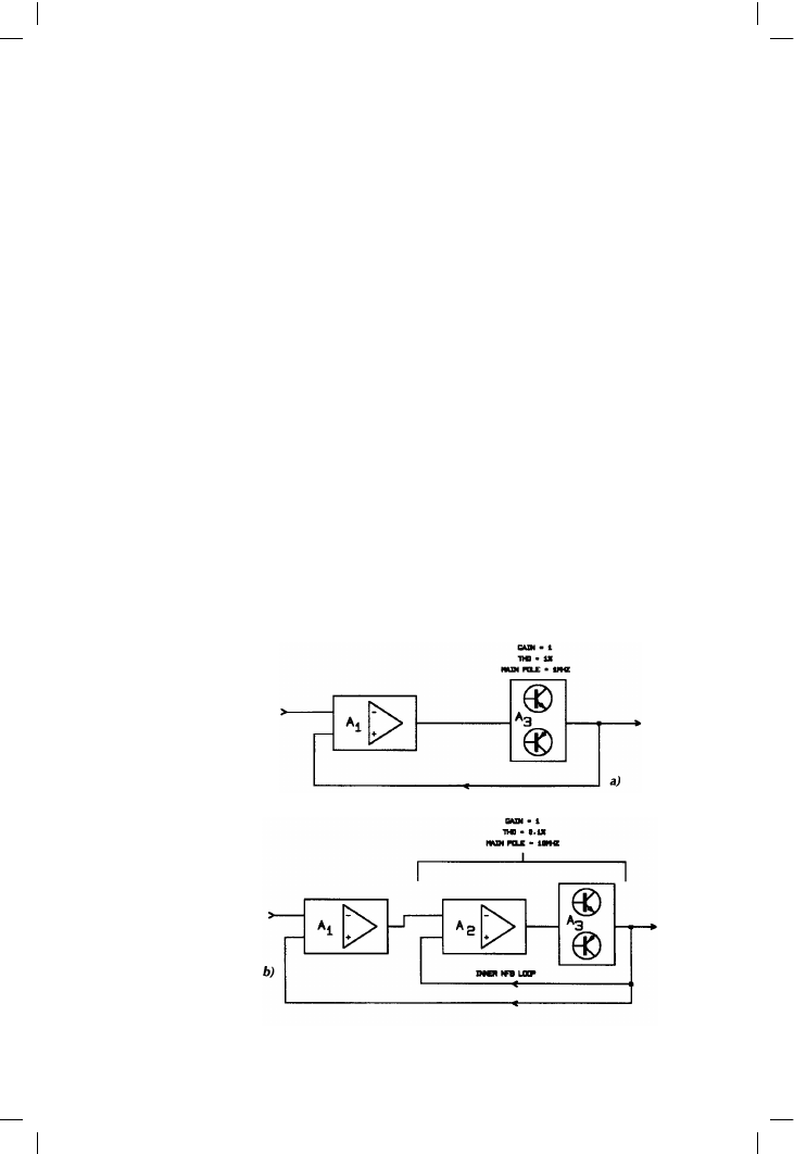
Suppose that bloc A1 (Figure 7.2a) is a Distortionless small-signal amplifier
providing all the open-loop gain and so including the dominant pole. A3 is
a unity-gain output stage with its own main pole at 1 MHz and distortion of
1% under given conditions; this 1 MHz pole puts a firm limit on the amount
of global NFB that can be safely applied. Figure 7.2b shows a nested-
187
Figure 7.2a
Normal single-loop
global negative
feedback
Figure 7.2b
Nested feedback

Audio Power Amplifier Design Handbook
feedback version; an extra gain-bloc A2 has been added, with local
feedback around the output stage. A2 has the modest gain of 20 dB so there
is a good chance of stability when this loop is closed to bring the gain of A3
+ A2 back to unity. A2 now experiences 20 dB of NFB, bringing the
distortion down to 0.1%, and raising the main pole to 10 MHz, which
should allow the application of 20 dB more global NFB around the overall
loop that includes A1. We have thus decreased the distortion that exists
before global NFB is applied, and simultaneously increased the amount of
NFB that can be safely used, promising that the final linearity could be very
good indeed. For another theoretical example see Pernici et al
[6]
.
Real-life examples of this technique in power amps are not easy to find, but it
is widely used in op-amps. Many of us were long puzzled by the way that the
much-loved 5534 maintained such low THD up to high frequencies.
Contemplation of its enigmatic entrails appears to reveal a three-gain-stage
design with an inner Miller loop around the third stage, and an outer Miller
loop around the second and third stages; global NFB is then applied
externally around the whole lot. Nested Miller compensation has reached its
apotheosis in CMOS opamps – the present record appears
[7]
to be three
nested Miller loops plus the global NFB; don’t try this one at home. More
details on the theory of nested feedback can be found in Scott and Spears
[8]
.
Two-pole compensation
Two-pole compensation is well-known as a technique for squeezing the
best performance from an op-amp
[9], [10]
, but it has rarely been applied to
power amplifiers; the only example I know is found in Widlar
[5]
. An extra
HF time constant is inserted in the Cdom path, giving an open-loop gain
curve that initially falls at almost 12 dB/octave, but which gradually reverts
to 6 dB/octave as frequency continues to increase. This reversion is
arranged to happen well before the unity loop-gain line is reached, and so
stability should be the same as for the conventional dominant-pole scheme,
but with increased negative feedback over part of the operational
frequency range. The faster gain roll-off means that the maximum amount
of feedback can be maintained up to a higher frequency. There is no
measurable mid-band peak in the closed-loop response.
It is right to feel nervous about any manoeuvre that increases the NFB
factor; power amplifiers face varying conditions and it is difficult to be sure
that a design will always be stable under all circumstances. This makes
designers rather conservative about compensation, and I approached this
technique with some trepidation. However, results were excellent with no
obvious reduction in stability. See Figure 7.4 for the happy result of
applying this technique to the Class-B amplifier seen in Figure 7.5.
The simplest way to implement two-pole compensation is shown in Figure
7.1d, with typical values. Cp1 should have the same value as it would for
188

Compensation, slew-rate, and stability
stable single-pole compensation, and Cp2 should be at least twice as big;
Rp is usually in the region 1k–10k. At intermediate frequencies Cp2 has an
impedance comparable with Rp, and the resulting extra time-constant
causes the local feedback around the VAS to increase more rapidly with
frequency, reducing the open-loop gain at almost 12 dB/octave. At HF the
impedance of Rp is high compared with Cp2, the gain slope asymptotes
back to 6 dB/octave, and then operation is the same as conventional
dominant-pole, with Cdom equal to the series capacitance combination.
So long as the slope returns to 6 dB/octave before the unity loop-gain
crossing occurs, there seems no obvious reason why the Nyquist stability
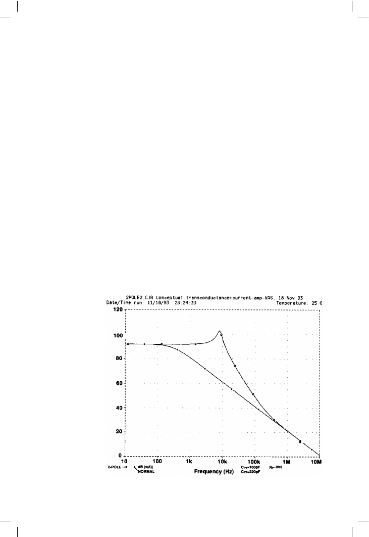
should be impaired. Figure 7.3 shows a simulated two-pole open-loop gain
plot for realistic component values; Cp2 should be at least twice Cp1 so the
gain falls back to the 6 dB/octave line before the unity loop-gain line is
crossed. The potential feedback factor has been increased by more than
20 dB from 3 kHz to 30 kHz, a region where THD tends to increase due to
falling NFB. The open-loop gain peak at 8 kHz looks extremely dubious,
but I have so far failed to detect any resulting ill-effects in the closed-loop
behaviour.
There is however a snag to the approach shown here, which reduces the
linearity improvement. Two-pole compensation may decrease open-loop
linearity at the same time as it raises the feedback factor that strives to
correct it. At HF, Cp2 has low impedance and allows Rp to directly load the
VAS collector to ground; as we have seen, this worsens VAS linearity.
189
Figure 7.3
The open-loop gain
plot for two-pole
compensation with
realistic component
values