ВУЗ: Казахская Национальная Академия Искусств им. Т. Жургенова
Категория: Учебное пособие
Дисциплина: Не указана
Добавлен: 03.02.2019
Просмотров: 17418
Скачиваний: 18

Audio Power Amplifier Design Handbook
obtained if all seven of the distortion mechanisms are properly addressed;
Distortions 1–4 are determined by the circuit design, but the remaining three
depend critically on physical layout and grounding topology.
It is hard to beat a well-gilded lily, and so Figure 6.19 shows the startling
results of applying 2-pole compensation to the basic amplifier; C3 remains
100 pF, while CP2 was 220 pF and Rp 1k (see Figure 7.1d, page 185). The
180
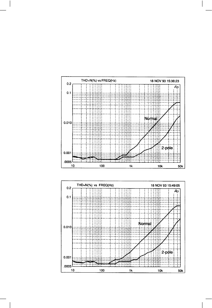
Figure 6.20
Class-B amplifier with
simple quasi-
complementary output.
Lower trace is for two-
pole compensation
Figure 6.21
Class-B amplifier with
quasi-comp plus
Baxandall diode
output. Lower trace is
the two-pole case

The output stage II
extra global NFB does its work extremely well, the 10 kHz THD dropping
to 0.0015%, while the 1 kHz figure can only be guessed at. There were no
unusual signs of instability, but as always unusual compensation schemes
require careful testing. It does appear that a Blameless amplifier with 2-pole
compensation takes us close to the long-sought goal of the Distortionless
Amplifier.
The basic Blameless EF amplifier was experimentally rebuilt with three
alternative output stages; the simple quasi-complementary, the quasi-
Baxandall, and the CFP. The results for both single and two-pole
compensation are shown in Figures 6.20, 6.21, and 6.22. The simple quasi-
complementary generates more crossover distortion, as expected, and the
181
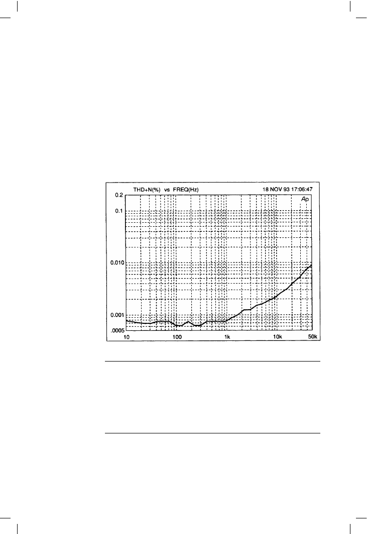
Figure 6.22
Class-B amplifier with
complementary
feedback pair (CFP)
output stage. Normal
compensation only
Table 6.1
Class-B amplifier
performance
Power output:
50 W rms into 8 !
Distortion:
Below 0.0006% at 1 kHz and 50 W/8 !
Below 0.006% at 10 kHz
Slew-rate:
Approx. 35 V/µsec
Noise:
91 dBu at the output
EIN:
117 dBu (referred to input)
Freq Response:
+0, –0.5 dB over 20 Hz–20 kHz
(Most of the AP plots in this book were obtained from an amplifier similar to Figure
6.16, though with higher supply rails and so greater power capability. The main
differences were the use of a cascode-VAS with a buffer, and a CFP output to
minimise distracting quiescent variations. Measurements at powers above
100 W/8 ! used a version with two paralleled output devices.)

Audio Power Amplifier Design Handbook
quasi-Baxandall version is not a lot better, probably due to remaining
asymmetries around the crossover region. The CFP gives even lower
distortion than the original EF-II output, with Figure 6.19 showing only the
result for single-pole compensation; in this case the improvement with two-
pole was marginal and the trace is omitted for clarity.
References
1. Ball, G Distorting Power Supplies Electronics & Wireless World, Dec
1990, p. 1084.
2. Cherry, A New Distortion Mechanism in Class-B Amplifiers Journ. Audio
Eng. Soc. May 1981, p. 327.
3. Baxandall, P Private communication, 1995.
4. Self, D Distortion In Power Amplifiers Series in Electronics & Wireless
World, Aug 93 to March 94.
5. Self, D An Advanced Preamplifier Wireless World, Nov 1976, p. 43.
182

7
Compensation, slew-rate,
and stability
Frequency compensation in general
The compensation of an amplifier is the tailoring of its open-loop gain and
phase characteristics so that is dependably stable when the global feedback
loop is closed.
It must be said straight away that compensation is a thoroughly misleading
word to describe the subject of this chapter. It implies that one problematic
influence is being balanced out by another opposing force, when in fact it
means the process of tailoring the open-loop gain and phase of an amplifier
so that it is satisfactorily stable when the global feedback loop is closed.
The derivation of the word is historical, going back to the days when all
servomechanisms were mechanical, and usually included an impressive
Watt governor pirouetting on top of the machinery.
An amplifier requires compensation because its basic open-loop gain is still
high at frequencies where the internal phase-shifts are reaching 180
degrees. This turns negative feedback into positive at high frequencies, and
causes oscillation, which in audio amplifiers can be very destructive. The
way to prevent this is to ensure that the loop gain falls to below unity before
the phase-shift reaches 180 degrees; oscillation therefore cannot develop.
Compensation is therefore vital simply because it makes the amplifier
stable; there are other considerations, however, because the way in which
the compensation is applied has a major effect on the closed-loop
distortion behaviour.
The distortion performance of an amplifier is determined not only by open-
loop linearity, but also the negative feedback factor applied when the loop
is closed; in most practical circumstances doubling the NFB factor halves
the distortion. So far I have assumed that open-loop gain falls at 6 dB/octave
due to a single dominant pole, with the amount of NFB permissible at HF
183

Audio Power Amplifier Design Handbook
being set by the demands of HF stability. We have seen that this results in
the distortion from a Blameless amplifier consisting almost entirely of
crossover artefacts, because of their high-order and hence high frequency.
Audio amplifiers using more advanced compensation are rather rare.
However, certain techniques do exist, and are described later.
This book sticks closely to conventional topologies, because even
apparently commonplace circuitry has proven to have little-known aspects,
and to be capable of remarkable linearity. This means the classical three-
stage architecture circuit with transconductance input, transimpedance
VAS, and unity-gain output stage. Negative feedback is applied globally,
but is smoothly transferred by Cdom to be local solely to the VAS as
frequency increases. Other configurations are possible; a two-stage
amplifier with transconductance input and unity-gain output is an
intriguing possibility – this is common in CMOS op-amps – but is probably
ill-suited to power-amp impedances. Another architecture with a voltage-
gain input stage is described in Chapter 11, and see Otala
[1]
for an
eccentric four-stage amplifier with a low open-loop gain of 52 dB (due to
the dogged use of local feedback) and only 20 dB of global feedback. Most
of this chapter relates only to the conventional three-stage structure.
Dominant-pole compensation
Dominant-pole compensation is the simplest kind, though its action is
subtle. Simply take the lowest pole to hand (P1), and make it dominant, i.e.
so much lower in frequency than the next pole P2 that the total loop-gain
(i.e. the open-loop gain as reduced by the attenuation in the feedback
network) falls below unity before enough phase-shift accumulates to cause
HF oscillation. With a single pole, the gain must fall at 6 dB/octave,
corresponding to a constant 90-degree phase shift. Thus the phase margin
will be 90 degrees, giving good stability.
Figure 7.1a shows the traditional Miller method of creating a dominant
pole. The collector pole of TR4 is lowered by adding the external Miller-
capacitance Cdom to that which unavoidably exists as the internal Cbc of
the VAS transistor. However, there are some other beneficial effects; Cdom
causes pole-splitting, in which the pole at TR2 collector is pushed up in
frequency as P1 is moved down – most desirable for stability. Simultane-
ously the local NFB through Cdom linearises the VAS.
Assuming that input-stage transconductance is set to a plausible 5 mA/V,
and stability considerations set the maximal 20 kHz open-loop gain to
50 dB, then from Equations 3.1–3.3 on pages 61 and 62, Cdom must be
125 pF. This is more than enough to swamp the internal capacitances of the
VAS transistor, and is a practical real-life value.
The peak current that flows in and out of this capacitor for an output of 20 V
rms at 20 kHz, is 447 µA. Since the input stage must sink Cdom current
184