ВУЗ: Казахская Национальная Академия Искусств им. Т. Жургенова
Категория: Учебное пособие
Дисциплина: Не указана
Добавлен: 03.02.2019
Просмотров: 17424
Скачиваний: 18

Audio Power Amplifier Design Handbook
However, if Cp2 and Rp are correctly proportioned the overall reduction in
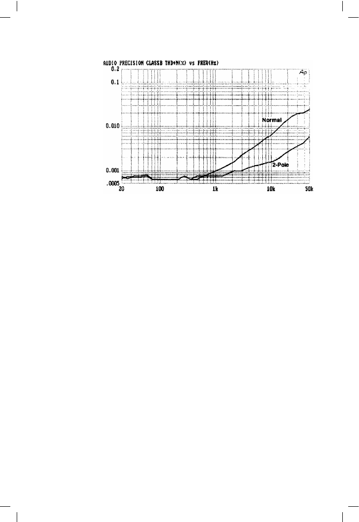
distortion is dramatic and extremely valuable. When two-pole compensa-
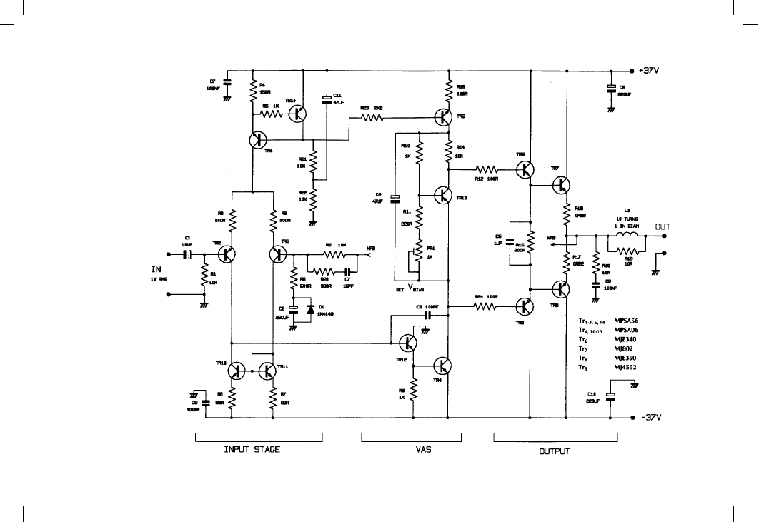
tion was added to the amplifier circuit shown in Figure 7.5, the crossover
glitches on the THD residual almost disappeared, being partially replaced
by low-level second harmonic which almost certainly results from VAS
loading. The positive slew-rate will also be slightly reduced.
This looks like an attractive technique, as it can be simply applied to an
existing design by adding two inexpensive components. If Cp2 is much
larger than Cp1, then adding/removing Rp allows instant comparison
between the two kinds of compensation. Be warned that if an amplifier is
prone to HF parasitics then this kind of compensation may worsen them.
Output networks
The usual output networks for a power amplifier are shown in Figure 7.6,
with typical values. They comprise a shunt Zobel network, for stability into
inductive loads, and a series output inductor/damping resistor for stability
into capacitive loads.
Amplifier output impedance
The main effect of output impedance is usually thought to be its effect on
Damping Factor. This is wrong, as explained in Chapter 1. Despite this
demonstration of its irrelevance, I will refer to Damping Factor here, to
show how an apparently impressive figure dwindles as more parts of the
speaker-cable system are included.
190
Figure 7.4
Distortion reduction
with two-pole
compensation

191
Figure 7.5
The Class-B amplifier
from Chapter 6. At the
simplest level the
maximum slew-rate is
defined by the current
source TR1 and the
value of Cdom

Audio Power Amplifier Design Handbook
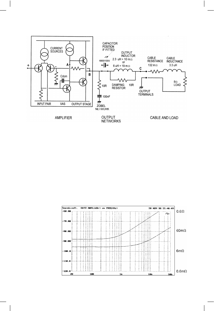
Figure 7.6 shows a simplified amplifier with Zobel network and series
output inductor, plus simple models of the connecting cable and speaker
load. The output impedance of a solid-state amplifier is very low if even a
modest amount of global NFB is used. I measured a Blameless Class-B
amplifier similar to Figure 7.5 with the usual NFB factor of 29 dB at 20 kHz,
increasing at 6 dB/octave as frequency falls. Figure 7.7 shows the output
impedance at point B before the output inductor, measured by injecting a
10 mA signal current into the output via a 600 ! resistance.
192
Figure 7.6
The amplifier-cable-speaker system. Simplified amplifier with Zobel network and damped output inductor, and
a resistive load. Cable resistance and inductance values are typical for a 5 metre length
Figure 7.7
Output impedance of
a Blameless amplifier,
with and without
6 µH output inductor.
Adding the inductor
(upper trace)
increases both the
flat LF output
impedance, due to
its series resistance,
and the rising HF
impedance

Compensation, slew-rate, and stability
The low-frequency output impedance is approx 9 m! (an 8 ! Damping
Factor of 890). To put this into perspective, one metre of thick 32/02
equipment cable (32 strands of 0.2 mm diameter) has a resistance of
16.9 m!. The internal cabling resistance in an amplifier can equal or
exceed the output impedance of the amplifier itself at LF.
Output impedance rises at 6 dB/octave above 3 kHz, as global NFB falls off,
reaching 36 m! at 20 kHz. The 3 kHz break frequency does not correspond
with the amplifier dominant pole frequency, which is much lower at
around 10 Hz.
The closed-loop output impedance of any amplifier is set by the open-loop
output impedance and the negative feedback factor. The output impedance
is not simply the output impedance of the output stage alone, because the
latter is driven from the VAS, so there is a significant and frequency-varying
source impedance at point A in Figure 7.6.
When the standard EF and CFP stages are driven from a zero-impedance
source, in both cases the raw output impedance is in the region of
150–180 m!. This assumes the emitter resistors Re are 0.1 !. Increasing Re
to 0.22 ! increases output impedance to the range 230–280 m!, showing
that these resistors in fact make up most of the output impedance. The
output devices and drivers have little influence.
If the average open-loop output impedance is 200 m!, and the NFB factor
at 20 kHz is 29 dB, or 28 times, we would expect a closed-loop output
impedance of approximately 200/28, which is 7 m!. Since it is actually
about 33 m! at this frequency, there is clearly more going on than simple
theory implies. In a real amplifier the output stage is not driven from a zero
impedance, but a fairly high one that falls proportionally with frequency;
for my Blameless Class-B design it falls from 3 k ! at 1 kHz to about 220 !
at 20 kHz. A 220 ! source impedance produces an open-loop output
impedance of about 1 !, which when reduced by a factor of 28 when
global feedback is applied, gives 35 m!. This is close to the value
measured at 20 kHz at point B in Figure 7.6.
All of these measured closed-loop output impedances are very low
compared with the other impedances in the amp-cable-speaker system. It
would appear they can in most cases be ignored.
The Blameless amplifier design shown on page 176 has an output inductor
of approx. 6 µH; the aim is absolutely guaranteed stability into all
capacitative loads, and the inductance is therefore at the high end of the
permissible range. This is limited by the HF roll-off into the lowest load
resistance to be driven. This substantial component comprises 20 turns of
1.5 mm diam. copper wire, wound to 1 inch diameter, and has a DC
resistance of 19 m!. This small extra resistance raises the flat section of the
impedance plot to 24 m!, and in fact dominates the LF output impedance
193

Audio Power Amplifier Design Handbook
as measured at the amplifier terminals (point C). It also sharply reduces the
notional Damping Factor from 890 to 330.
Naturally the inductance of the coil pushes the rising portion of the
impedance curve higher. The output impedance now starts to rise from
700 Hz, still at 6 dB per octave, reaching 0.6 ! at 20 kHz. See Figure 7.7.
Minimising amplifier output impedance
This issue is worth considering, not because it optimises speaker dynamics,
which it doesn’t, but because it minimises frequency response variations due
to varying speaker impedance. There is also, of course, specmanship to be
considered.
It is clear from Figure 7.7 that the output impedance of a generic amplifier
will very probably be less than the inductor resistance, so the latter should be
attended to first. Determine the minimum output inductance for stability
with capacitive loads, because lower inductance means fewer turns of wire
and less resistance. Some guidance on this is given in the next section. Note,
however, that the inductance of the usual single-layer coil varies with the
square of the number of turns, so halving the inductance only reduces the
turns, and hence the series resistance, by root-two. The coil wire must be as
thick as the cost/quality tradeoffs allow.
It is also desirable to minimise the resistance of the amplifier internal wiring,
and to carefully consider any extra resistance introduced by output relays,
speaker switching, etc. When these factors have been reduced as far as cost
and practicality allow, it is likely that the output impedance of the actual
amplifier will still be the smallest component of the total.
Zobel networks
All power amplifiers except for the most rudimentary kinds include a Zobel
network in their arrangements for stability. This simple but somewhat
enigmatic network comprises a resistor and capacitor in series from the
amplifier output rail to ground. It is always fitted on the inside (i.e. upstream)
of the output inductor, though a few designs have a second Zobel network
after the output inductor; the thinking behind this latter approach is obscure.
The resistor approximates to the expected load impedance, and is usually
between 4.7 and 10 !. The capacitor is almost invariably 100 nF, and these
convenient values and their constancy in the face of changing amplifier
design might lead one to suppose that they are not critical; in fact experiment
suggests that the real reason is that the traditional values are just about right.
The function of the Zobel network (sometimes also called a Boucherot cell)
is rarely discussed, but is usually said to prevent too inductive a reactance
being presented to the amplifier output by a loudspeaker voice-coil, the
implication being that this could cause HF instability. It is intuitively easy to
194