ВУЗ: Казахская Национальная Академия Искусств им. Т. Жургенова
Категория: Учебное пособие
Дисциплина: Не указана
Добавлен: 03.02.2019
Просмотров: 17395
Скачиваний: 18

Class-G power amplifiers
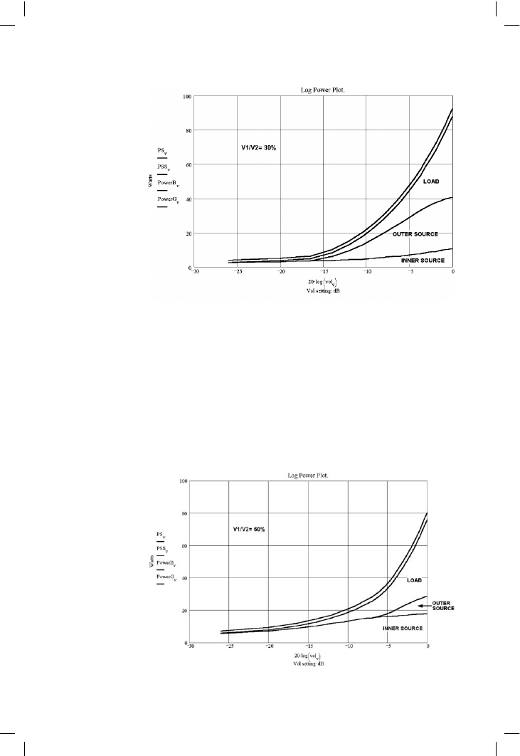
In Figure 10.4 the lower area represents the power dissipated in the inner
devices and the larger area just above represents that in the outer devices;
there is only one area for each because in Class-B and Class-G only one
side of the amplifier conducts at a time. Outer device dissipation is zero
below the rail-switching threshold at –15 dB below maximum output. The
total device dissipation at full output power is reduced from 48 W in Class-
B to 40 W, which may not appear at first to be a very good return for
doubling the power transistors and drivers.
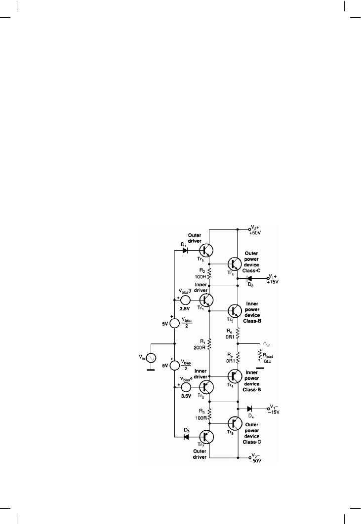
Figure 10.5 shows the same PPD but with ±V2 = 50 V and ±V1 = 30 V, i.e.
with V1/V2 set to 60%. The low-voltage region now extends up to –6 dB ref
295
Figure 10.4
Power partition
diagram for Class-G
with V1/V2 = 30%.
Signal has a
triangular PDF. X-axis
is volume; outer
devices dissipate
nothing until –15 dB
is reached
Figure 10.5
Power partition
diagram for Class-G
with V1/V2 = 60%.
Triangular PDF.
Compared with
Figure 10.4, the
inner devices
dissipate more and
the outer devices
almost nothing
except at maximum
volume

Audio Power Amplifier Design Handbook
full power, but the inner device dissipation is higher due to the higher V1
rail voltages. The result is that total device power at full output is reduced
from 48 W in Class-B to 34 W, which is a definite improvement. The
efficiency figure is highly sensitive to the way the ratio of rail voltages
compares with the signal characteristics. Domestic hi-fi amplifiers are not
operated at full volume all the time, and in real life the lower option for the
V1 voltage is likely to give lower general dissipation. I do not suggest that
V1/V2 = 30% is the optimum lower-rail voltage for all situations, but it
looks about right for most domestic hi-fi.
Practicalities
In my time I have wrestled with many ‘new and improved’ output stages
that proved to be anything but. When faced with a new and intriguing
possibility, I believe the first thing to do is sketch out a plausible circuit such
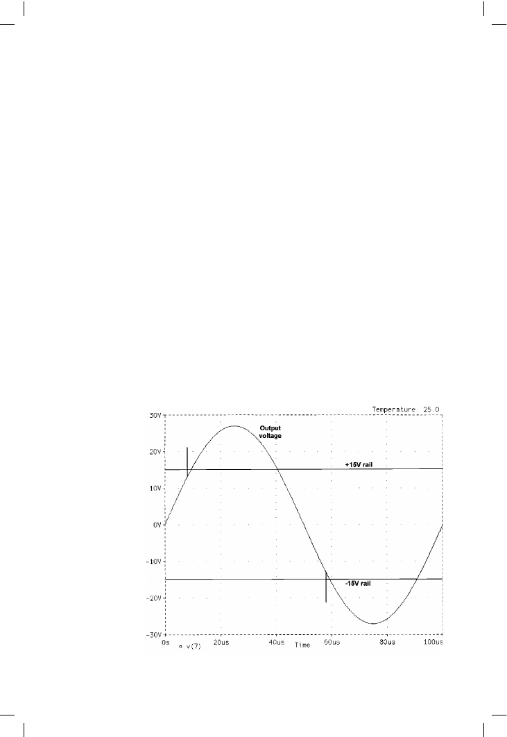
as Figure 10.1 and see if it works in SPICE simulation. It duly did.
The next stage is to build it, power it from low supply rails to minimise any
resulting explosions, and see if it works for real at 1 kHz. This is a bigger
step than it looks.
SPICE simulation is incredibly useful but it is not a substitute for testing a
real prototype. It is easy to design clever and complex output stages that
work beautifully in simulation but in reality prove impossible to stabilise at
high frequencies. Some of the most interesting output-triple configurations
seem to suffer from this.
The final step – and again it is a bigger one than it appears – is to prove real
operation at 20 kHz and above. Again it is perfectly possible to come up
with a circuit configuration that either just does not work at 20 kHz, due to
limitations on power transistor speeds, or is provoked into oscillation or
other misbehaviour that is not set off by a 1 kHz testing.
Only when these vital questions are resolved is it time to start considering
circuit details, and assessing just how good the amplifier performance is
likely to be.
The biasing requirements
The output stage bias requirements are more complex than for Class-B. Two
extra bias generators Vbias3, Vbias4 are required to make TR6 turn on
before TR3 runs out of collector voltage. These extra bias voltages are not
critical, but must not fall too low, or become much too high. Should these
bias voltages be set too low, so the outer devices turn on too late, then the
Vce across TR3 becomes too low, and its current sourcing capability is
reduced. When evaluating this issue bear in mind the lowest impedance
load the amplifier is planned to drive, and the currents this will draw from
the output devices. Fixed Zener diodes of normal commercial tolerance are
quite accurate and stable enough for setting Vbias3 and Vbias4.
296

Class-G power amplifiers
Alternatively, if the bias voltage is set too low, then the outer transistors will
turn on too early, and the heat dissipation in the inner power devices
becomes greater than it need be for correct operation. The latter case is
rather less of a problem so if in doubt this bias should be chosen to be on
the high side rather than the low.
The original Hitachi circuit
[1]
put Zeners in series with the signal path to the
inner drivers to set the output quiescent bias, their voltage being subtracted
from the main bias generator which was set at 10 V or so, a much higher
voltage than usual (see Figure 10.6). SPICE simulation showed me that the
presence of Zener diodes in the forward path to the inner power devices gave
poor linearity, which is not exactly a surprise. There is also the problem that
the quiescent conditions will be affected by changes in the Zener voltage.
The 10 V bias generator, if it is the usual Vbe multiplier, will have much too
high a temperature coefficient for proper thermal tracking.
I therefore rearrange the biasing as in Figure 10.1. The amplifier forward
path now goes directly to the inner devices, and the two extra bias voltages
297
Figure 10.6
The original Hitachi
Class-G biasing
system, with inner
device bias derived by
subtracting Vbias3, 4
from the main bias
generator

Audio Power Amplifier Design Handbook
are in the path to the outer devices; since these do not control the output
directly, the linearity of this path is of little importance. The Zeners are out
of the forward path and the bias generator can be the standard sort. It must
be thermally coupled to the inner power devices; the outer ones have no
effect on the quiescent conditions.
The linearity issues of series Class-G
Series Class-G has often had its linearity called into question because of
difficulties with supply-rail commutation. Diodes D3, D4 must be power
devices capable of handling a dozen amps or more, and conventional
silicon rectifier diodes that can handle such currents take a long time to
turn off due to their stored charge carriers. This has the following unhappy
effect: when the voltage on the cathode of D3 rises above V1, the diode
tries to turn off abruptly, but its charge carriers sustain a brief but large
reverse current as they are swept from its junction. This current is supplied
by TR6, attempting as an emitter-follower to keep its emitter up to the right
voltage. So far all is well.
However, when the diode current ceases, TR6 is still conducting heavily,
due to its own charge-carrier storage. The extra current it turned on to feed
D3 in reverse now goes through TR3 collector, which accepts it because of
TR3’s low Vce, and passes it onto the load via TR3 emitter and Re.
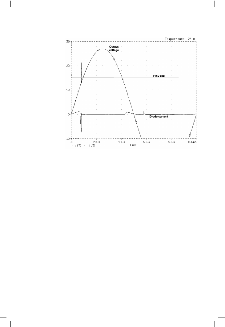
This process is readily demonstrated by a SPICE commutation transient
simulation; see Figures 10.7 and 10.8. Note there are only two of these
298
Figure 10.7
Spikes due to charge
storage of
conventional diodes,
simulated at 10 kHz.
They only occur
when the diodes turn
off, so there are only
two per cycle. These
spikes disappear
completely when
Schottky diodes are
used in the SPICE
model

Class-G power amplifiers
events per cycle – not four, as they only occur when the diodes turn off. In
the original Hitachi design this problem was reportedly tackled by using
fast transistors and relatively fast gold-doped diodes, but according to
Sampei et al
[2]
this was only partially successful.
It is now simple to eradicate this problem. Schottky power diodes are
readily available, as they were not in 1976, and are much faster due to their
lack of minority carriers and charge storage. They have the added
advantage of a low forward voltage drop at large currents of 10 A or more.
The main snag is a relatively low reverse withstand voltage, but fortunately
in Class-G usage the commutating diodes are only exposed at worst to the
difference between V2 and V1, and this only when the amplifier is in its
low power domain of operation. Another good point about Schottky power
diodes is that they do appear to be robust; I have subjected 50 amp
Motorola devices to 60 amps-plus repeatedly without a single failure. This
is a good sign. The spikes disappear completely from the SPICE plot if the
commutating diodes are Schottky rectifiers. Motorola MBR5025L diodes
capable of 50 A and 25 PIV were used in simulation.
The static linearity
SPICE simulation shows in Figure 10.9 that the static linearity (i.e. that
ignoring dynamic effects like diode charge-storage) is distinctly poorer than
for Class-B. There is the usual Class-B gain-wobble around the crossover
299
Figure 10.8
A close-up of the
diode transient.
Diode current rises as
output moves away
from zero, then
reverses abruptly as
charge carriers are
swept out by reverse-
biasing. The spike on
the output voltage is
aligned with the
sudden stop of the
diode reverse current