ВУЗ: Казахская Национальная Академия Искусств им. Т. Жургенова
Категория: Учебное пособие
Дисциплина: Не указана
Добавлен: 03.02.2019
Просмотров: 17393
Скачиваний: 18

Audio Power Amplifier Design Handbook
region, exactly the same size and shape as for conventional Class-B, but
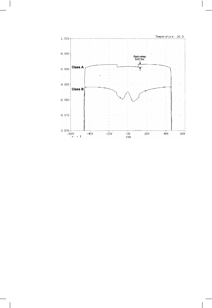
also there are now gain-steps at ±16 V. The result with the inner devices
biased into push-pull Class-A is also shown, and proves that the gain-steps
are not in any way connected with crossover distortion. Since this is a DC
analysis the gain-steps cannot be due to diode switching-speed or other
dynamic phenomena, and Early Effect was immediately suspected. (Early
Effect is the increase in collector current when the collector voltage
increases, even though the Vbe remains constant.) When unexpected
distortion appears in a SPICE simulation of this kind, and effects due to
finite transistor beta and associated base currents seem unlikely, a most
useful diagnostic technique is to switch off the simulation of Early Effect for
each transistor in turn. In SPICE transistor models the Early Effect can be
totally disabled by setting the parameter VAF to a much higher value than
the default of 100, such as 50,000. This experiment demonstrated in short
order that the gain-steps were caused wholly by Early Effect acting on both
inner drivers and inner output devices. The gain-steps are completely
abolished. When TR6 begins to act, TR3 Vce is no longer decreasing as the
output moves positive, but substantially constant as the emitter of Q6
moves upwards at the same rate as the emitter of Q3. This has the effect of
a sudden change in gain, which naturally degrades the linearity.
This effect appears to occur in drivers and output devices to the same
extent. It can be easily eliminated in the drivers by powering them from the
outer rather than the inner supply rails. This prevents the sudden changes
300
Figure 10.9
SPICE simulation
shows variations in
the incremental gain
of an EF-type Class-G
series output stage.
The gain-steps at
transition (at ±16 V)
are due to Early
Effect in the
transistors. The Class-
A trace is the top
one, with Class-B
optimal below. Here
the inner driver
collectors are
connected to the
switched inner rails,
i.e. the inner power
device collectors, as
in Figure 10.1

Class-G power amplifiers
301
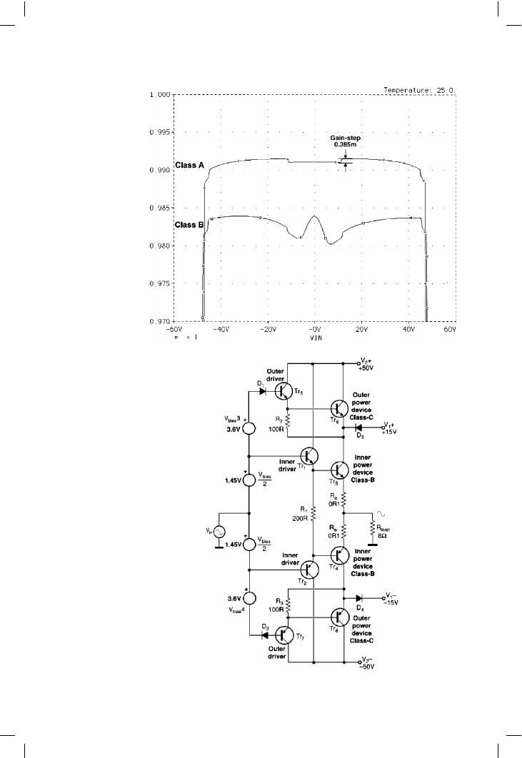
Figure 10.10
Connecting the inner
driver collectors to
the outer V2 rails
reduces Early Effect
non-linearities in
them, and halves the
transition gain-steps
Figure 10.11
A Class-G output stage
with the drivers
powered from the outer
supply rails

Audio Power Amplifier Design Handbook
in the rate in which driver Vce varies. The improvement in linearity is seen
in Figure 10.10, where the gain-steps have been halved in size. The
resulting circuit is shown in Figure 10.11. Driver power dissipation is
naturally increased by the increased driver Vce, but this is such a small
fraction of the power consumed that the overall efficiency is not
significantly reduced. It is obviously not practical to apply the same method
to the output devices, because then the low-voltage rail would never be
used and the amplifier is no longer working in Class-G. The small-signal
stages naturally have to work from the outer rails to be able to generate the
full voltage swing to drive the output stage.
We have now eliminated the commutating diode glitches, and halved the
size of the unwanted gain-steps in the output stage. With these improve-
ments made it is practical to proceed with the design of a Class-G amplifier
with midband THD below 0.002%.
Practical Class-G design
The Class-G amplifier design expounded here uses very similar small-signal
circuitry to the Blameless Class-B power amplifier, as it is known to
generate very little distortion of its own. If the specified supply voltages of
±50 and ±15 V are used, the maximum power output is about 120 W into
8 !, and the rail-switching transition occurs at 28 W.
This design incorporates various techniques described in this book, and
closely follows the Blameless Class-B amp described on page 176, though
some features derive from the Trimodal (page 279) and Load Invariant
(page 134) amplifiers. A notable example is the low-noise feedback
network, complete with its option of input bootstrapping to give a high
impedance when required. Single-slope VI limiting is incorporated for
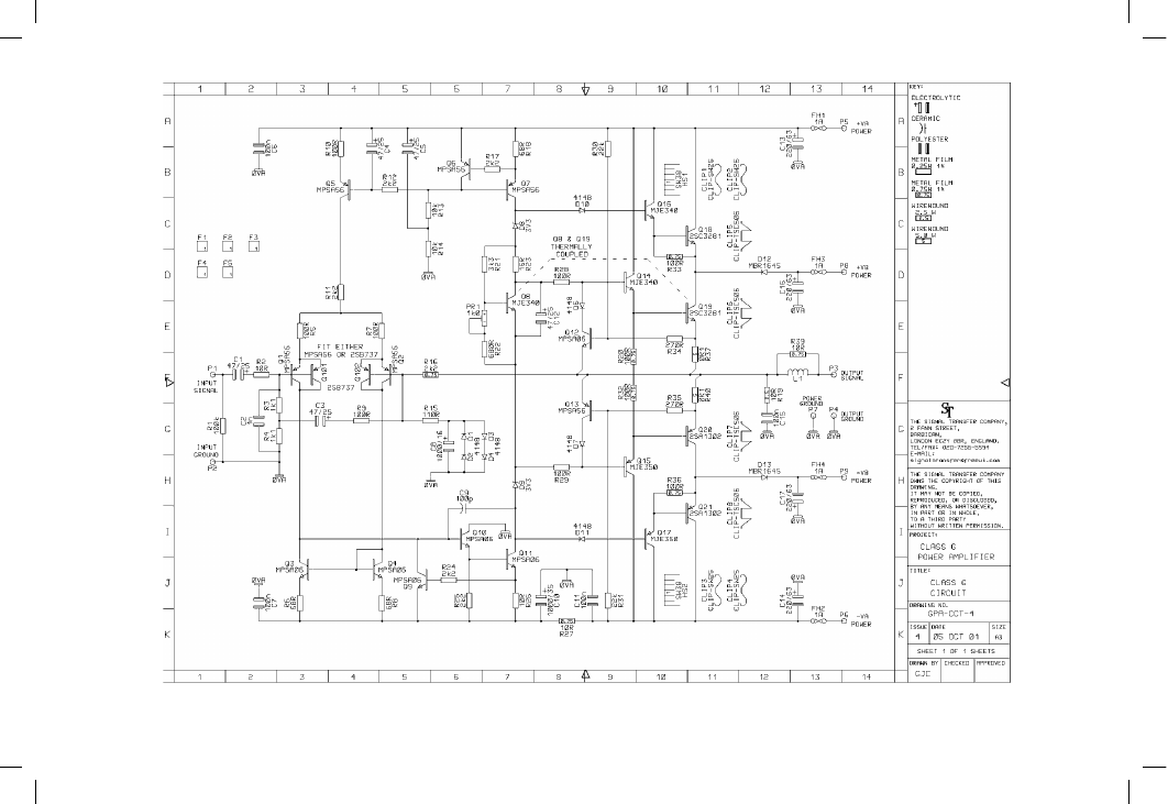
overload protection; this is implemented by Q12, 13. Figure 10.12 shows
the circuit.
As usual in my amplifiers the global NFB factor is a modest 30 dB at
20 kHz.
Controlling small-signal distortion
The distortion from the small-signal stages is kept low by the same methods
as for the other amplifier designs in this book, and so this is only dealt with
briefly here. The input stage differential pair Q1, 2 is given local feedback
by R5 and R7 to delay the onset of third-harmonic Distortion 1. Internal r
e
variations in these devices are minimised by using an unusually high tail
current of 6 mA. Q3, 4 are a degenerated current-mirror that enforces
accurate balance of the Q1, 2 collector currents, preventing the production
of second-harmonic distortion. The input resistance (R3 + R4) and feedback
resistance R16 are made equal and made unusually low, so that base
302

303
Figure 10.12
The circuit diagram of the Class-G amplifier

Audio Power Amplifier Design Handbook
current mismatches stemming from input device beta variations give a
minimal DC offset. Vbe mismatches in Q1 and Q2 remain, but these are
much smaller than the effects of Ib. Even if Q1 and Q2 are high-voltage
types with relatively low beta, the DC offset voltage at the output should be
kept to less than ±50 mV. This is adequate for all but the most demanding
applications. This low-impedance technique eliminates the need for
balance presets or DC servo systems, which is most convenient.
A lower value for R16 implies a proportionally lower value for R15 to keep
the gain the same, and this reduction in the total impedance seen by Q2
improves noise performance markedly. However, the low value of R3 plus
R4 at 2k2 gives an input impedance which is not high enough for many
applications.
There is no problem if the amplifier is to have an additional input stage,
such as a balanced line receiver. Proper choice of opamp will allow the
stage to drive a 2k2 load impedance without generating additional
distortion. Be aware that adding such a stage – even if it is properly
designed and the best available opamps are used – will degrade the signal-
to-noise ratio significantly. This is because the noise generated by the
power amplifier itself is so very low – equivalent to the Johnson noise of a
resistor of a few hundred ohms – that almost anything you do upstream will
degrade it seriously.
If there is no separate input stage then other steps must be taken. What we
need at the input of the power amplifier is a low DC resistance, but a high
AC resistance; in other words we need either a 50 henry choke or recourse
to some form of bootstrapping. There is to my mind no doubt about the way
to go here, so bootstrapping it is. The signal at Q2 base is almost exactly the
same as the input, so if the mid-point of R3 and R4 is driven by C3, so far
as input signals are concerned R3 has a high AC impedance. When I first
used this arrangement I had doubts about its high-frequency stability, and
so added resistor R9 to give some isolation between the bases of Q1 and
Q2. In the event I have had no trouble with instability, and no reports of any
from the many constructors of the Trimodal and Load-Invariant designs,
which incorporate this option.
The presence of R9 limits the bootstrapping factor, as the signal at R3–R4
junction is thereby a little smaller than at Q2 base, but it is adequate. With
R9 set to 100R, the AC input impedance is raised to 13k, which should be
high enough for almost all purposes. Higher values than this mean that an
input buffer stage is required.
The value of C8 shown (1000 µF) gives an LF roll-off in conjunction with
R15 that is –3 dB at 1.4 Hz. The purpose is not impossibly extended sub-
bass, but the avoidance of a low-frequency rise in distortion due to non-
linearity effects in C8. If a 100 µF capacitor is used here the THD at 10 Hz
worsens from <0.0006% to 0.0011%, and I regard this as unacceptable
304