ВУЗ: Казахская Национальная Академия Искусств им. Т. Жургенова
Категория: Учебное пособие
Дисциплина: Не указана
Добавлен: 03.02.2019
Просмотров: 17390
Скачиваний: 18

Class-G power amplifiers
aesthetically – if not perhaps audibly. This is not the place to define the low-
frequency bandwidth of the system – this must be done earlier in the signal
chain, where it can be properly implemented with more accurate non-
electrolytic capacitors. The protection diodes D1 to D4 prevent damage to
C2 if the amplifier suffers a fault that makes it saturate in either direction;
it looks like an extremely dubious place to put diodes but since they
normally have no AC or DC voltage across them no measurable or
detectable distortion is generated.
The Voltage-Amplifier-Stage (VAS) Q11 is enhanced by emitter-follower
Q10 inside the Miller-compensation loop, so that the local negative
feedback that linearises the VAS is increased. This effectively eliminates
VAS non-linearity. Thus increasing the local feedback also reduces the VAS
collector impedance, so a VAS-buffer to prevent Distortion 4 (loading of
VAS collector by the non-linear input impedance of the output stage) is not
required. Miller capacitor Cdom is relatively big at 100 pF, to swamp
transistor internal capacitances and circuit strays, and make the design
predictable. The slew rate calculates as 40 V/µsec use in each direction.
VAS collector-load Q7 is a standard current source.
Almost all the THD from a Blameless amplifier derives from crossover
distortion, so keeping the quiescent conditions optimal to minimise this is
essential. The bias generator for an EF output stage, whether in Class-B or
Class-G, is required to cancel out the Vbe variations of four junctions in
series; those of the two drivers and the two output devices. This sounds
difficult, because the dissipation in the two types of devices is quite
different, but the problem is easier than it looks. In the EF type of output
stage the driver dissipation is almost constant as power output varies, and
so the problem is reduced to tracking the two output device junctions. The
bias generator Q8 is a standard Vbe-multiplier, with R23 chosen to
minimise variations in the quiescent conditions when the supply rails
change. The bias generator should be in contact with the top of one of the
inner output devices, and not the heatsink itself. This position gives much
faster and less attenuated thermal feedback to Q8. The VAS collector circuit
incorporates not only bias generator Q8 but also the two Zeners D8, D9
which determine how early rail-switching occurs as the inner device
emitters approach the inner (lower) voltage rails.
The output stage was selected as an EF (emitter-follower) type as this is
known to be less prone to parasitic or local oscillations than the CFP
configuration, and since this design was to the same extent heading into the
unknown it seemed wise to be cautious where possible. R32 is the usual
shared emitter resistor for the inner drivers. The outer drivers Q16 and Q17
have their own emitter resistors R33 and R36, which have their usual role
of establishing a reasonable current in the drivers as they turn on, to
increase driver transconductance, and also in speeding up turn-off of the
outer output devices by providing a route for charge-carriers to leave the
output device bases.
305

Audio Power Amplifier Design Handbook
As explained above, the inner driver collectors are connected to the outer
rails to minimise the gain-steps caused by the abrupt change in collector
voltage when rail transition occurs.
Deciding the size of heatsink required for this amplifier is not easy,
mainly because the heat dissipated by a Class-G amplifier depends very
much on the rail voltages chosen and the signal statistics. A Class-B
design giving 120 W into 8R would need a heatsink with thermal
resistance of the order of 1°C/W (per channel); a good starting point for
a Class-G version giving the same power would be about half the size,
i.e. 2°C/W. The Schottky commutating diodes do not require much
heatsinking, as they conduct only intermittently and have a low forward
voltage drop. It is usually convenient to mount them on the main
heatsink, even if this does mean that most of the time they are being
heated rather than cooled.
C15 and R38 make up the usual Zobel network. The coil L1, damped by
R39, isolates the amplifier from load capacitance. A component with 15 to
20 turns at 1 inch diameter should work well; the value of inductance for
stability is not all that critical.
The performance
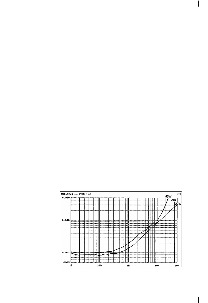
Figure 10.13 shows the THD at 20 W/50 W (into 8 !) and I think this
demonstrates at once that the design is a practical competitor for Class-B
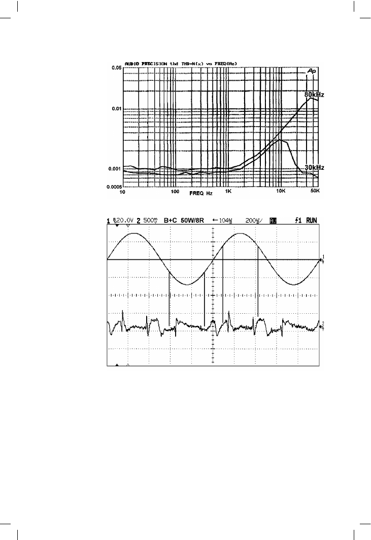
amplifiers. Compare these results with the upper trace of Figure 10.14,
taken from a Blameless Class-B amplifier at 50 W, 8 !. Note the lower trace
of Figure 10.14 is for 30 kHz bandwidth, used to demonstrate the lack of
distortion below 1 kHz; the THD data above 30 kHz is in this case
meaningless as all the harmonics are filtered out. All the Class-G plots here
306
Figure 10.13
THD versus
frequency, at 20 W
(below transition) and
50 W into an 8 !
load. The joggle
around 8 kHz is due
to a cancellation of
harmonics from
crossover and
transition. 80 kHz
bandwidth

Class-G power amplifiers
are taken at 80 kHz to make sure any high-order glitching is properly
measured.
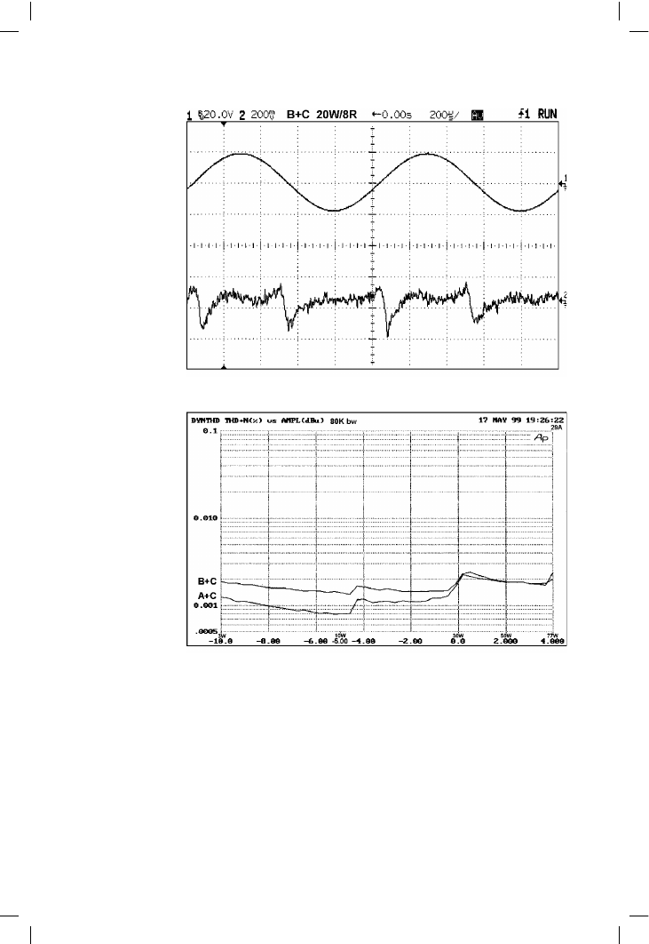
Figure 10.15 shows the actual THD residual at 50 W output power. The
glitches from the gain-steps are more jagged than the crossover dis-
turbances, as would be expected from the output stage gain plot in Figures
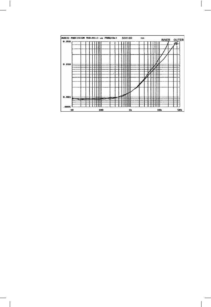
10.9, 10.11. Figure 10.16 confirms that at 20 W, below transition, the
residual is indistinguishable from that of a Blameless Class-B amplifier; in
this region, where the amplifier is likely to spend most of its time, there are
no compromises on quality.
307
Figure 10.14
THD versus frequency
for a Blameless
Class-B amplifier at
50 W, 8 !
Figure 10.15
The THD residual
waveform at 50 W
into 8 !. This residual
may look rough, but
in fact it had to be
averaged eight times
to dig the glitches
and crossover out of
the noise; THD is
only 0.0012%. The
vertical lines show
where transition
occurs

Audio Power Amplifier Design Handbook
Figure 10.17 shows THD versus level, demonstrating how THD increases
around 28 W as transition begins. The steps at about 10 W are nothing to do
with the amplifier – they are artefacts due to internal range-switching in the
measuring system.
Figure 10.18 shows for real the benefits of powering the inner drivers from
the outer supply rails. In SPICE simulation (see above) the gain-steps were
roughly halved in size by this modification, and Figure 10.18 duly confirms
that the THD is halved in the HF region, the only area where it is
sufficiently clear of the noise floor to be measured with any confidence.
308
Figure 10.16
The THD residual
waveform at 20 W
into 8 !, below
transition. Only
crossover artefacts
are visible as there is
no rail-switching
Figure 10.17
THD versus level,
showing how THD
increases around
28 W as transition
begins. Class-A + C
is the lower and
Class-B + C the
upper trace

Class-G power amplifiers
Deriving a new kind of amplifier: Class-A + C
A conventional Class-B power amplifier can be almost instantly converted
to push-pull Class-A simply by increasing the bias voltage to make the
required quiescent current flow. This is the only real circuit change, though
naturally major increases in heatsinking and power-supply capability are
required for practical use. Exactly the same principle applies to the Class-G
amplifier. Recently I suggested a new and much more flexible system for
classifying amplifier types
[6]
and here it comes in very handy. Describing
Class-G operation as Class-B + C immediately indicates that only a bias
increase is required to transform it into Class-A + C, and a new type of
amplifier is born. This amplifier configuration combines the superb
linearity of classic Class-A up to the transition level, with only minor
distortion artefacts occurring at higher levels, as demonstrated for Class-B
+ C above. Using Class-A means that the simple Vbe-multiplier bias
generator can be replaced with precise negative feedback control of the
quiescent current, as implemented in the Trimodal amplifier in this book.
There is no reason why an amplifier could not be configured as a Class-G
Trimodal, i.e. manually switchable between Classes A and B. That would
indeed be an interesting machine.
In Figure 10.19 is shown the THD plot for such an A + C amplifier working
at 20 W and 30 W into 8 !. At 20 W the distortion is very low indeed, no
higher than a pure Class-A amplifier. At 30 W the transition gain-steps
appear, but the THD remains very well controlled, and no higher than a
Blameless Class-B design. Note that as in Class-B, when the THD does start
to rise it only does so at 6 dB/octave. The quiescent current was set to
1.5 amps.
309
Figure 10.18
THD plot of real
amplifier driving
50 W into 8 !. Rails
were ±40 and
±25 V. Distortion at
HF is halved by
connecting the inner
drivers to the outer
supply rails rather
than the inner rails