ВУЗ: Казахская Национальная Академия Искусств им. Т. Жургенова
Категория: Учебное пособие
Дисциплина: Не указана
Добавлен: 03.02.2019
Просмотров: 17389
Скачиваний: 18

Audio Power Amplifier Design Handbook
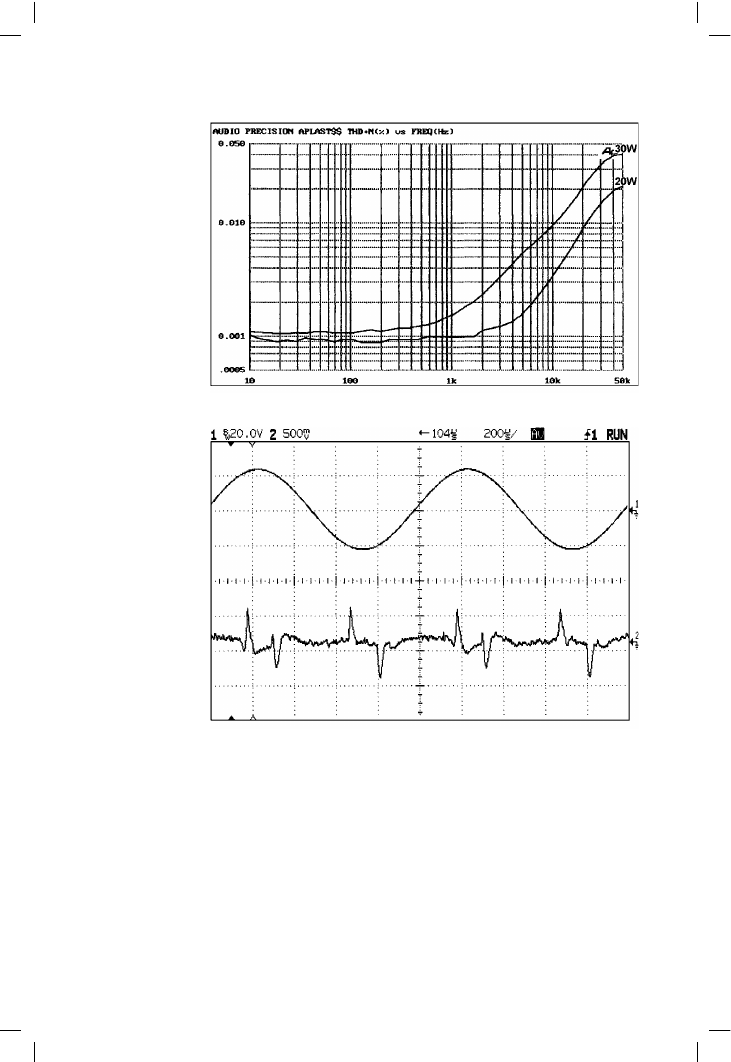
Figure 10.20 reveals the THD residual during A + C operation. There are
absolutely no crossover artefacts, and the small disturbances that do occur
happen at such a high signal level that I really do think it is safe to assume
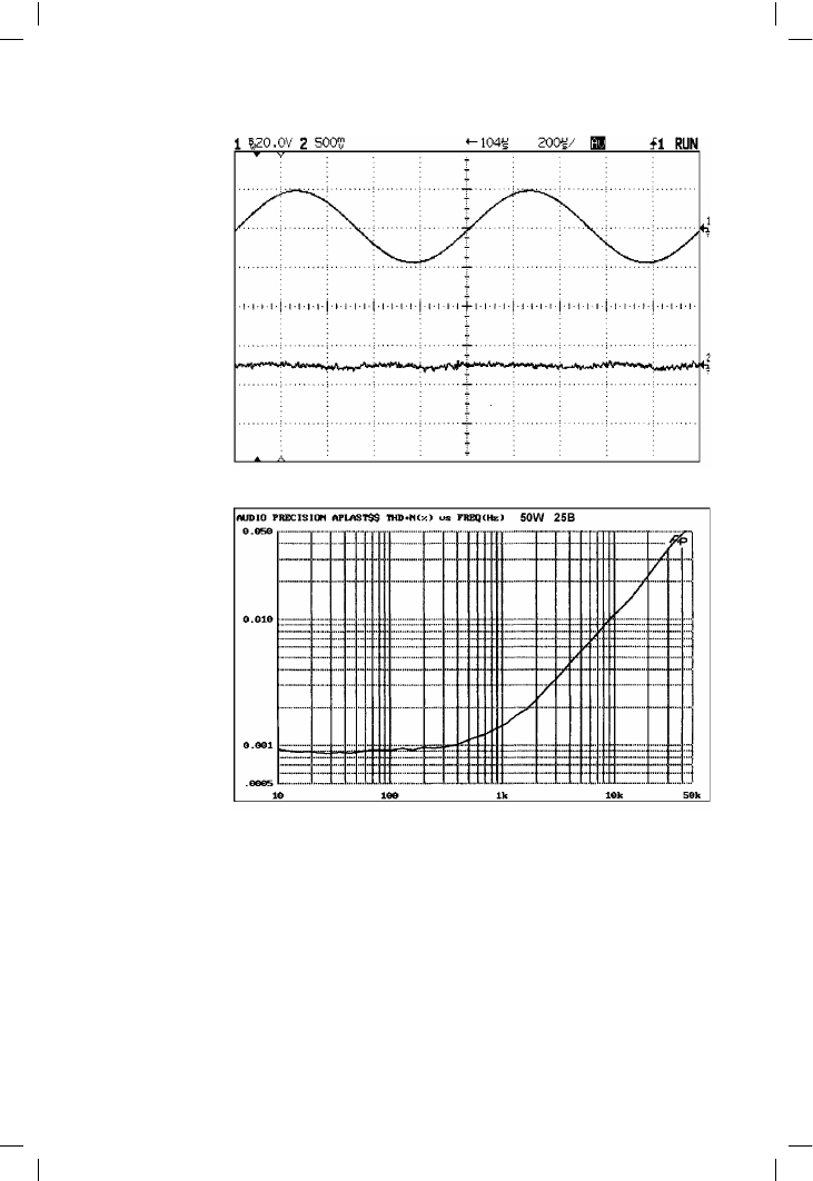
they could never be audible. Figure 10.21 shows the complete absence of
artefacts on the residual when this new type of amplifier is working below
transition; it gives pure Class-A linearity. Finally, Figure 10.22 gives the
THD when the amplifier is driving the full 50 W into 8 !; as before the A
+ C THD plot is hard to distinguish from Class-B, but there is the immense
advantage that there is no crossover distortion at low levels, and no critical
bias settings.
310
Figure 10.19
The THD plot of the
Class-A + C amplifier
(30 W and 20 W
into 8 !). Inner
drivers powered from
outer rails
Figure 10.20
The THD residual
waveform of the
Class-A + C amplifier
above transition, at
30 W into 8 !.
Switching artefacts
are visible but not
crossover distortion

Class-G power amplifiers
Adding two-pole compensation
I have previously shown elsewhere in this book that amplifier distortion can
be very simply reduced by changes to the compensation; which means a
scheme more sophisticated than the near-universal dominant pole method.
It must be borne in mind that any departure from the conventional 6 dB/
octave-all-the-way compensation scheme is likely to be a move away from
unconditional stability. (I am using this phrase in its proper meaning; in
Control Theory unconditional stability means that increasing open-loop
gain above a threshold causes instability, but the system is stable for all
311
Figure 10.21
The THD residual
waveform plot of the
Class-A + C amplifier
(20 W into 8 !)
Figure 10.22
The THD plot of the
Class-A + C amplifier
(50 W into 8 !).
Inner drivers
powered from outer
rails

Audio Power Amplifier Design Handbook
lower values. Conditional Stability means that lower open-loop gains can
also be unstable.)
A conditionally stable amplifier may well be docile and stable into any
conceivable reactive load when in normal operation, but shows the cloven
hoof of oscillation at power-up and power-down, or when clipping. This is
because under these conditions the effective open-loop gain is reduced.
Class-G distortion artefacts are reduced by normal dominant-pole feedback
in much the same way as crossover non-linearities, i.e. not all that
effectively, because the artefacts take up a very small part of the cycle and
are therefore composed of high-order harmonics. Therefore a compensa-
tion system that increases the feedback factor at high audio frequencies will
be effective on switching artefacts, in the same way that it is for crossover
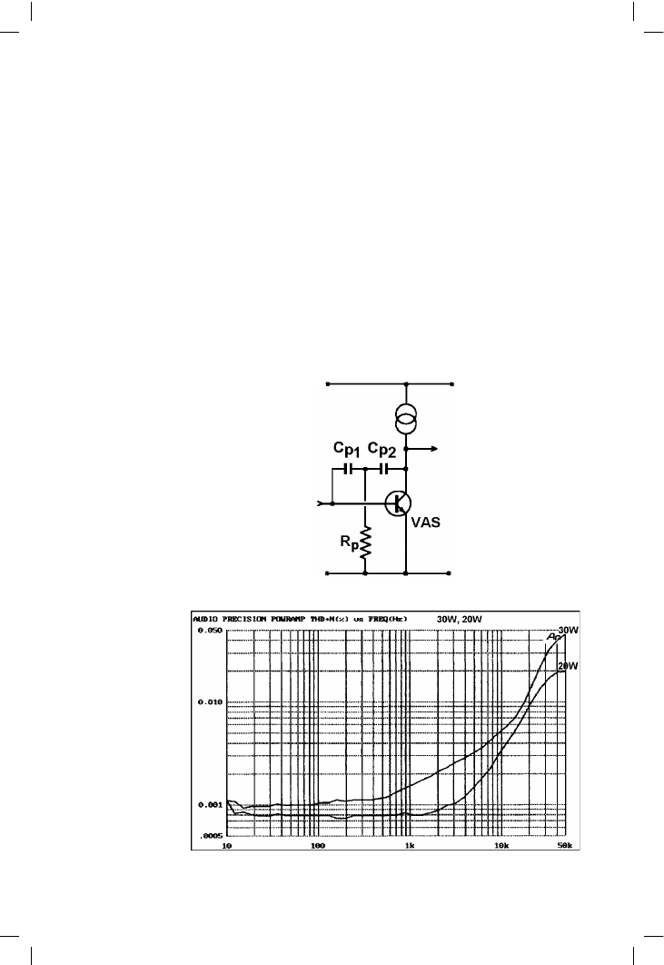
distortion. The simplest way to implement two-pole circuit compensation is
shown in Figure 10.23. Further details are given on page 188.
312
Figure 10.23
The circuit
modification for two-
pole compensation
Figure 10.24
The THD plot for B +
C operation with
two-pole
compensation (20 W
and 30 W into 8 !).
Compare with
Figures 10.13
(B + C) and 10.19
(A + C)

Class-G power amplifiers
The results of two-pole compensation for B + C are shown in Figure 10.24;
comparing it with Figure 10.13 (the normally compensated B + C amplifier)
the above-transition (30 W) THD at 10 kHz has dropped from 0.008% to
0.005%; the sub-transition (20 W) THD at 10 kHz has fallen from 0.007%
to 0.003%. Comparisons have to be done at 10 kHz or thereabouts to
ensure there is enough to measure.
Now comparing the two-pole B + C amplifier with Figure 10.19 (the A + C
amplifier) the above-transition (30 W) THD at 10 kHz of the former is lower
at 0.005% compared with 0.008%. As I have demonstrated before, proper
use of two-pole compensation can give you a Class-B amplifier that is hard
to distinguish from Class-A – at least until you put your hand on the
heatsink.
Further variations on Class-G
This by no means exhausts the possible variations that can be played on
Class-G. For example, it is not necessary for the outer devices to operate
synchronously with the inner devices. So long as they turn on in time, they
can turn off much later without penalty except in terms of increased
dissipation. In so-called syllabic Class-G, the outer devices turn on fast but
then typically remain on for 100 msec or so to prevent glitching; see
Funada and Akiya
[7]
for one version. Given the good results obtained with
straight Class-G, this no longer seems a promising route to explore.
With the unstoppable advance of multichannel amplifier and powered sub-
woofers, Class-G is at last coming into its own. It has recently even
appeared in a Texas ADSL driver IC. I hope I have shown how to make it
work, and then how to make it work better. From the results of a Web
search done today, I would modestly suggest that this might be the lowest
distortion Class-G amplifier so far.
References
1. Self, D Self On Audio Newnes, ISBN 0–7506–4765–5, p. 347.
2. Sampei et al ‘Highest Efficiency and Super Quality Audio Amplifier
Using MOS Power FETs in Class-G Operation’ IEEE Trans on Consumer
Electronics, Vol CE–24, #3 Aug 1978, p. 300.
3. Feldman ‘Class-G High Efficiency Hi-Fi Amplifier’ Radio Electronics,
Aug 1976, p. 47.
4. Self, D Self On Audio Newnes, ISBN 0–7506–4765–5, p. 369.
5. Self, D Self On Audio Newnes, ISBN 0–7506–4765–5, p. 386.
6. Self, D Self On Audio Newnes, ISBN 0–7506–4765–5 p. 293.
7. Funada & Akiya ‘A Study of High-Efficiency Audio Power Amplifiers
Using a Voltage Switching Method’ Journ. Audio Eng. Soc. Vol 32 #10,
Oct 1984, p. 755.
313

11
FET output stages
The characteristics of power FETS
An FET is essentially a voltage-controlled device. So are BJTs, despite the
conventional wisdom that persists in regarding them as current-controlled.
They are not, even if BJT base currents are non-negligible.
The power FETs normally used are enhancement devices – in other words,
with no voltage between gate and source they remain off. In contrast, the
junction FETs found in small-signal circuitry are depletion devices,
requiring the gate to be taken negative of the source (for the most common
N-channel devices) to reduce the drain current to usable proportions.
(Please note that the standard information on FET operation is in many
textbooks and will not be repeated here.)
Power FETs have large internal capacitances, both from gate to drain, and
from gate to source. The gate-source capacitance is effectively boot-
strapped by the source-follower configuration, but the gate-drain capaci-
tance, which can easily total 2000 pF, remains to be driven by the previous
stage. There is an obvious danger that this will compromise the amplifier
slew-rate if the VAS is not designed to cope.
FETs tend to have much larger bandwidths than BJT output devices. My
own experience is that this tends to manifest itself as a greater propensity
for parasitic oscillation rather than anything useful, but the tempting
prospect of higher global NFB factors due to a higher output stage pole
remains. The current state of knowledge does not yet permit a definitive
judgement on this.
A great deal has been said on the thermal coefficients of the Vbias voltage.
It is certainly true that the temp coefficient at high drain currents is negative
314