ВУЗ: Казахская Национальная Академия Искусств им. Т. Жургенова
Категория: Учебное пособие
Дисциплина: Не указана
Добавлен: 03.02.2019
Просмотров: 17371
Скачиваний: 18

The general principles of power amplifiers
decreases. Large-signal THD worsens with 4 ! loads and worsens again at
2 !. The picture is complicated by dilatory switch-off in the relatively slow
output devices, ominously signalled by supply current increasing in the top
audio octaves.
Distortion four: VAS loading distortion
Loading of the VAS by the non-linear input impedance of the output stage.
When all other distortion sources have been attended to, this is the limiting
distortion factor at LF (say below 2 kHz); it is simply cured by buffering the
VAS from the output stage. Magnitude is essentially constant with
frequency, though overall effect in a complete amplifier becomes less as
frequency rises and feedback through Cdom starts to linearise the VAS.
Distortion five: rail decoupling distortion
Non-linearity caused by large rail-decoupling capacitors feeding the
distorted signals on the supply lines into the signal ground. This seems to be
the reason that many amplifiers have rising THD at low frequencies.
Examining one commercial amplifier kit, I found that rerouting the
decoupler ground-return reduced the THD at 20 Hz by a factor of three.
Distortion six: induction distortion
Non-linearity caused by induction of Class-B supply currents into the
output, ground, or negative-feedback lines. This was highlighted by
Cherry
[3]
but seems to remain largely unknown; it is an insidious distortion
that is hard to remove, though when you know what to look for on the THD
residual it is fairly easy to identify. I suspect that a large number of
commercial amplifiers suffer from this to some extent.
Distortion seven: NFB takeoff distortion
Non-linearity resulting from taking the NFB feed from slightly the wrong
place near where the power-transistor Class-B currents sum to form the
output. This may well be another very prevalent defect.
Distortion eight: capacitor distortion
Distortion, rising as frequency falls, caused by non-linearity in the input
DC-blocking capacitor or the feedback network capacitor. The latter is
more likely.
Non-existent distortions
Having set down what might be called The Eight Great Distortions, we
must pause to put to flight a few Paper Tigers . . . The first is common-mode
65

Audio Power Amplifier Design Handbook
distortion in the input stage, a spectre that haunts the correspondence
columns. Since it is fairly easy to make an amplifier with less than
<0.00065% THD (1 kHz) without paying any special attention to this it
cannot be too serious a problem.
Giovani Stochino and I have investigated this a little, and we have
independently found that if the common-mode voltage on the input pair is
greatly increased, then a previously negligible distortion mechanism is
indeed provoked. This CM increase is achieved by reducing the C/L gain to
between 1 and 2x; the input signal is much larger for the same output, and
the feedback signal must match it, so the input stage experiences a
proportional increase in CM voltage.
At present it appears that the distortion produced by this mechanism
increases as the square of the CM voltage. It therefore appears that the only
precautions required against common-mode distortion are to ensure that
the closed-loop gain is at least 5 times (which is no hardship, as it almost
certainly is anyway) and to use a tail current-source for the input pair.
The second distortion conspicuous by its absence in the list is the injection
of distorted supply-rail signals directly into the amplifier circuitry. Although
this putative mechanism has received a lot of attention
[4]
, dealing with
Distortion 5 above by proper grounding seems to be all that is required;
once more, if triple-zero THD can be attained using simple unregulated
supplies and without paying any attention to the Power Supply Rejection
Ratio beyond keeping the amplifier free from hum (which it reliably can be)
then there seems to be no problem. There is certainly no need for regulated
supply rails to get a good performance. PSRR does need careful attention if
the hum/noise performance is to be of the first order, but a little RC filtering
is usually all that is needed. This is dealt with in Chapter 8.
A third mechanism of very doubtful validity is thermal distortion,
allegedly induced by parameter changes in semiconductor devices whose
instantaneous power dissipation varies over a cycle. This would surely
manifest itself as a distortion rise at very low frequencies, but it simply
does not happen. There are several distortion mechanisms that can give a
THD rise at LF, but when these are eliminated the typical distortion trace
remains flat down to at least 10 Hz. The worst thermal effects would be
expected in Class-B output stages where dissipation varies wildly over a
cycle; however drivers and output devices have relatively large junctions
with high thermal inertia. Low frequencies are of course also where the
NFB factor is at its maximum. This contentious issue is dealt with at
greater length in Chapter 5.
To return to our list of the unmagnificent eight, note that only Distortion 3
is directly due to O/P stage non-linearity, though numbers 4–7 all result
from the Class-B nature of the typical output stage. Distortion 8 can happen
in any amplifier stage.
66

The general principles of power amplifiers
The performance of a standard amplifier
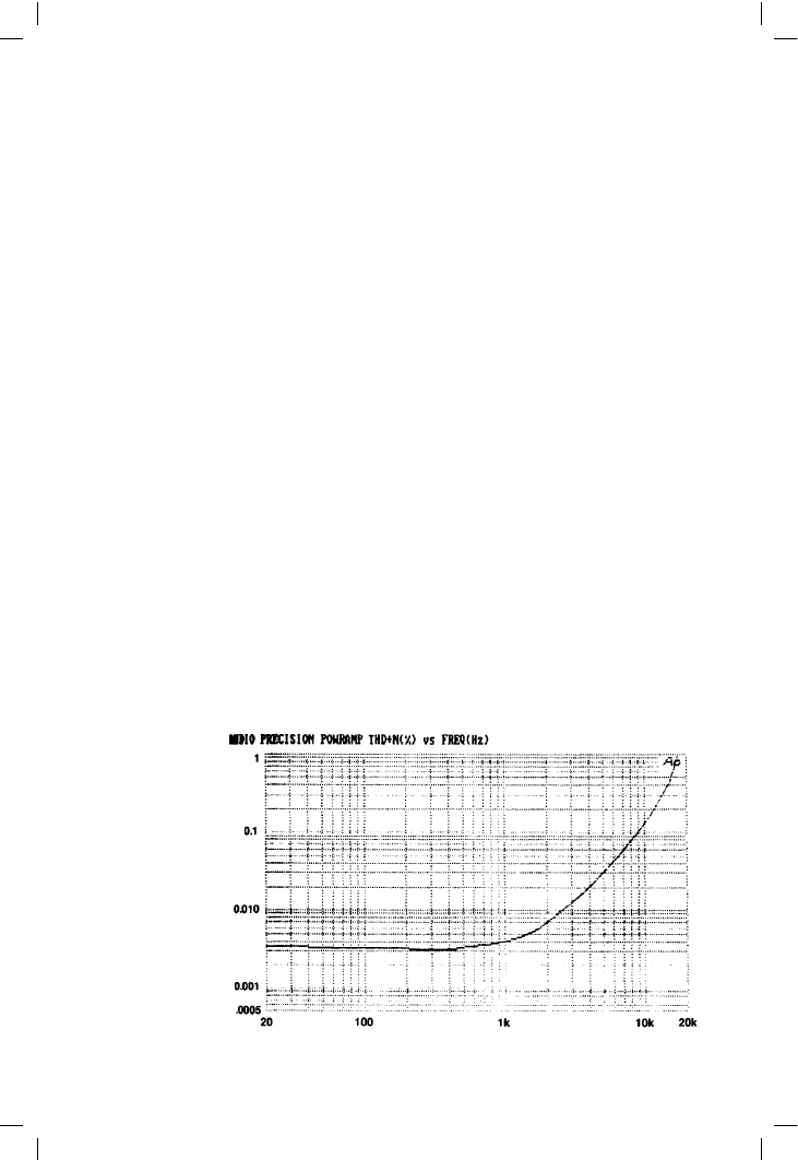
The THD curve for the standard amplifier is shown in Figure 3.3. As usual,
distortion increases with frequency, and as we shall see later, would give
grounds for suspicion if it did not. The flat part of the curve below 500 Hz
represents non-frequency-sensitive distortion rather than the noise floor,
which for this case is at the 0.0005% level. Above 500 Hz the distortion
rises at an increasing rate, rather than a constant number of dB/octave,
due to the combination of Distortions 1, 2, 3 and 4. (In this case
Distortions 5, 6 and 7 have been carefully eliminated to keep things
simple; this is why the distortion performance looks good already, and the
significance of this should not be overlooked.) It is often written that
having distortion constant across the audio band is a Good Thing; a most
unhappy conclusion, as the only practical way to achieve this with a
Class-B amplifier is to increase the distortion at LF, for example by
allowing the VAS to distort significantly.
It should now be clear why it is hard to wring linearity out of such a snake-
pit of contending distortions. A circuit-value change is likely to alter at least
2 of the distortion mechanisms, and probably change the o/l gain as well;
in the coming chapters I shall demonstrate how each distortion mechanism
can be measured and manipulated in isolation.
Open-loop linearity and how to determine it
Improving something demands measuring it, and thus it is essential to
examine the open-loop linearity of power-amp circuitry. This cannot be
done directly, so it is necessary to measure the NFB factor and calculate
open-loop distortion from closed-loop measurements. The closed-loop
gain is normally set by input sensitivity requirements.
67
Figure 3.3
The distortion
performance of the
Class-B amplifier in
Figure 3.1

Audio Power Amplifier Design Handbook
Measuring the feedback-factor is at first sight difficult, as it means
determining the open-loop gain. Standard methods for measuring op-amp
open-loop gain involve breaking feedback-loops and manipulating closed-
loop (c/l) gains, procedures that are likely to send the average power-
amplifier into fits. Nonetheless the need to measure this parameter is
inescapable, as a typical circuit modification – e.g. changing the value of
R2 – changes the open-loop gain as well as the linearity, and to prevent
total confusion it is essential to keep a very clear idea of whether an
observed change is due to an improvement in o/l linearity or merely
because the o/l gain has risen. It is wise to keep a running check on this as
work proceeds, so the direct method of open-loop gain measurement
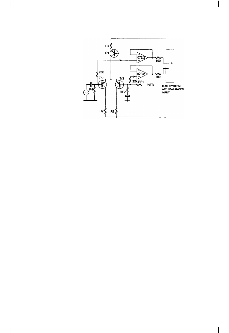
shown in Figure 3.4 was evolved.
Direct o/l gain measurement
The amplifier shown in Figure 3.1 is a differential amplifier, so its open-
loop gain is simply the output divided by the voltage difference between
the inputs. If output voltage is kept constant by providing a constant
swept-frequency voltage at the +ve input, then a plot of open-loop gain
versus frequency is obtained by measuring the error-voltage between the
inputs, and referring this to the output level. This gives an upside-down
plot that rises at HF rather than falling, as the differential amplifier
requires more input for the same output as frequency increases, but the
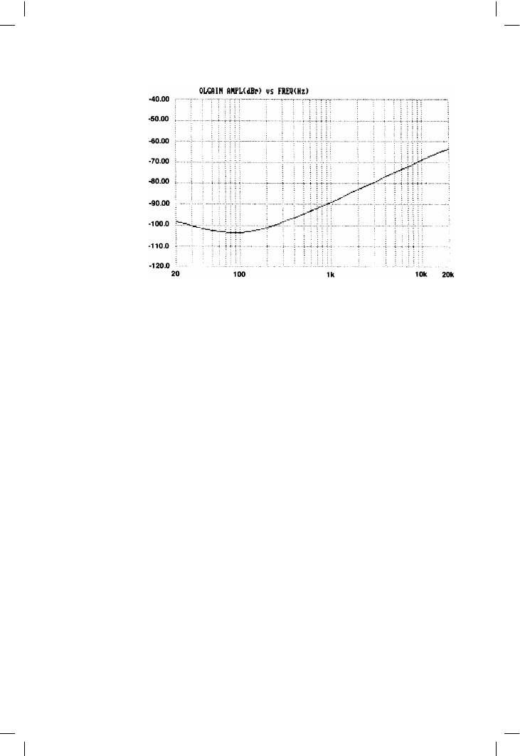
method is so quick and convenient that this can be lived with. Gain is
plotted in dB with respect to the chosen output level (+16 dBu in this
case) and the actual gain at any frequency can be read off simply by
dropping the minus sign. Figure 3.5 shows the plot for the amplifier in
Figure 3.1.
68
Figure 3.4
Test circuit for
measuring open-loop
gain directly. The
accuracy with which
high o/l gains can be
measured depends on
the testgear CMRR

The general principles of power amplifiers
The HF-region gain slope is always 6 dB/octave unless you are using
something special in the way of compensation, and by the Nyquist rules
must continue at this slope until it intersects the horizontal line
representing the feedback factor, if the amplifier is stable. In other words,
the slope is not being accelerated by other poles until the loop gain has
fallen to unity, and this provides a simple way of putting a lower bound
on the next pole P2; the important P2 frequency (which is usually
somewhat mysterious) must be above the intersection frequency if the
amplifier is seen to be stable.
Given test-gear with a sufficiently high Common-Mode-Rejection-Ratio
balanced input, the method of Figure 3.4 is simple; just buffer the
differential inputs from the cable capacitance with TL072 buffers, which
place negligible loading on the circuit if normal component values are
used. In particular be wary of adding stray capacitance to ground to the –ve
input, as this directly imperils amplifier stability by adding an extra
feedback pole. Short wires from power amplifier to buffer IC can usually be
unscreened as they are driven from low impedances.
The testgear input CMRR defines the maximum open-loop gain measur-
able; I used an Audio Precision System-1 without any special alignment of
CMRR. A calibration plot can be produced by feeding the two buffer inputs
from the same signal; this will probably be found to rise at 6 dB/octave,
being set by the inevitable input assymmetries. This must be low enough for
amplifier error signals to be above it by at least 10 dB for reasonable
accuracy. The calibration plot will flatten out at low frequencies, and may
even show an LF rise due to imbalance of the test-gear input-blocking
capacitors; this can make determination of the lowest pole P1 difficult, but
this is not usually a vital parameter in itself.
69
Figure 3.5
Open-loop gain
versus freq plot for
Figure 3.1. Note that
the curve rises as gain
falls, because the
amplifier error is the
actual quantity
measured