ВУЗ: Казахская Национальная Академия Искусств им. Т. Жургенова
Категория: Учебное пособие
Дисциплина: Не указана
Добавлен: 03.02.2019
Просмотров: 17394
Скачиваний: 18

Audio Power Amplifier Design Handbook
120
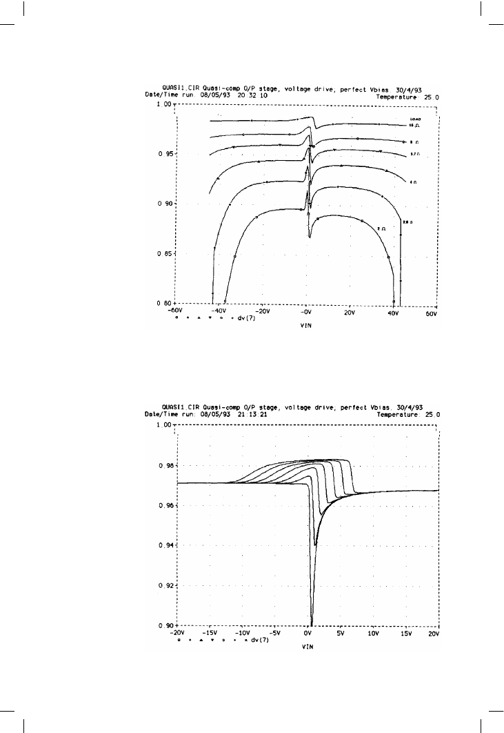
Figure 5.11
Quasi-complementary
large-signal gain vs
output
Figure 5.12
Quasi crossover region
+/–20 V, Vbias as
parameter

The output stage I
value of R1 in Figure 5.5c is not critical; making it about the same as Rc
seems to work well.
Triple-based output configurations
If we allow the use of three rather than two bipolar transistors in each half
of an output stage, the number of circuit permutations possible leaps
upwards, and I cannot provide even a rapid overview in the space
available. There are two possible advantages if output triples are used
correctly:
1 better linearity at high output voltages and currents,
2 more stable quiescent setting as the pre-drivers can be arranged to
handle very little power indeed, and to remain almost cold in use.
However, triples do not abolish crossover distortion, and they are, as
usually configured, incapable of reverse-biasing the output bases to
improve switchoff. Figure 5.6 shows three of the more useful ways to make
a triple output stage – all of those shown (with the possible exception of
Figure 5.6c, which I have just made up) have been used in commercial
designs, and Figure 5.6a will be recognised as the Quad-303 quasi-
complementary triple. The design of triples demands care, as the possibility
of local HF instability in each output half is very real.
Triple EF output stages
Sometimes it is necessary to use a triple output stage simply because the
currents flowing in the output stage are too big to be handled by two
transistors in cascade. If you are driving 2 ! or 1 ! loads, then typically
there will be multiple output devices in parallel. Providing the base current
for five or more output transistors, with their relatively low beta, will
usually be beyond the normal driver types, and it is common to use another
output device as the driver. This will hopefully have the power-handling
capability, but with this comes low beta once again. This means that the
driver base currents in turn become too large for a normal VAS stage to
source. There are two solutions – make the VAS capable of sourcing
hundreds of mA, or insert another stage of current – gain between VAS and
drivers. The latter is much easier, and the usual choice. These extra
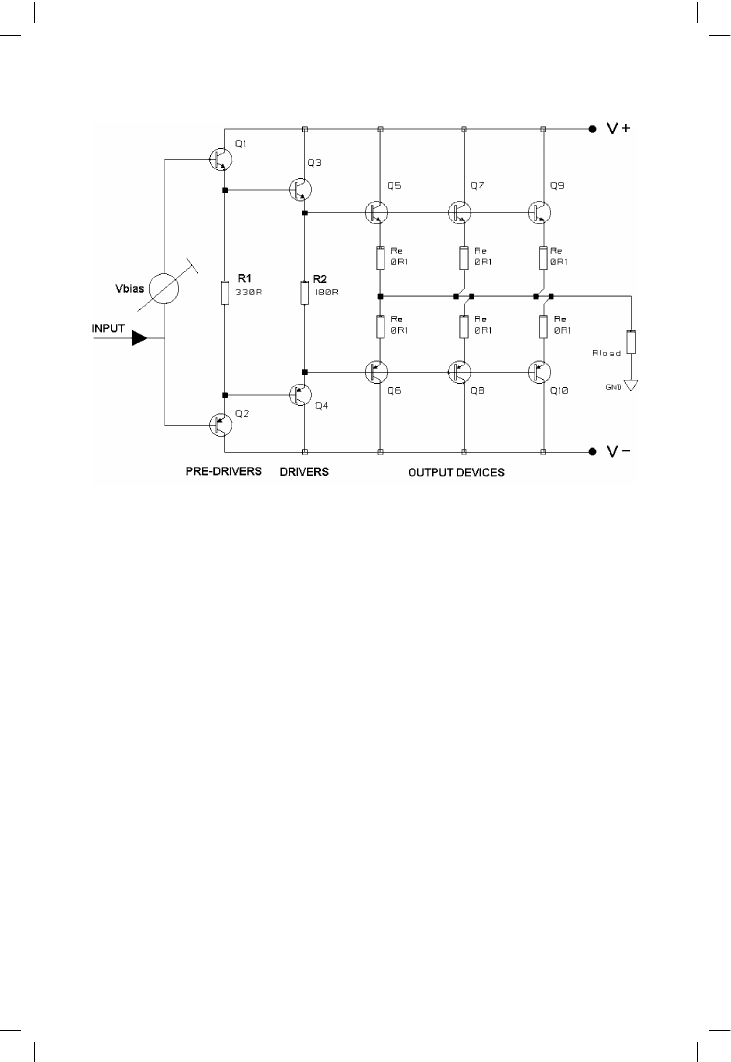
transistors are usually called the pre-drivers (see Figure 5.13).
In this circuit the pre-drivers dissipate relatively little power, and providing
they are medium-power devices such as those in a TO220 package it is
unlikely that they will need heatsinking to cope with the demands made on
them. There is, however, another reason to fit pre-drive heatsinks – or at
least make room at the layout stage so you have the option.
In Figure 5.13 there is about 1.2 V across R2, so Q3, 4 have to supply a
standing current of about 7 mA. This has no effect on the drivers as they are
121

Audio Power Amplifier Design Handbook
likely to be well cooled to deal with normal load demands. However, the
voltage across R1 is two Vbe’s higher, at 2.4 V, so the standing current
through it is actually higher at 7.3 mA. (The exact figures naturally depend
on the values for R1, R2 that are chosen, but it is difficult to make them
much higher than shown here without compromising the speed of high-
frequency turn-off.) The pre-drivers are usually small devices, and so they
are likely to get warm, and this leads to drift in the bias conditions after
switch-on. Adding heatsinks cannot eliminate this effect, but does usefully
reduce it.
In a triple-EF output stage like this the Vbias generator must produce
enough voltage to turn on six base-emitter junctions, plus the small
standing voltage Vq across the emitter resistors, totalling about 3.9 V in
practice. The Vbe of the bias transistor is therefore being multiplied by a
larger factor, and Vbias will drop more for the same temperature rise. This
should be taken into account, as it is easy with this kind of output stage to
come up with a bias generator that is overcompensated for temperature.
Distortion and its mechanisms
Subdividing Distortion 3 into Large-Signal Non-linearity, crossover, and
switchoff distortion provides a basis for judging which output stage is best.
The LSN is determined by both circuit topology and device characteristics,
122
Figure 5.13
A triple-EF output stage. Both pre-drivers and drivers have emitter-resistors

The output stage I
crossover distortion is critically related to quiescent-conditions stability,
and switchoff distortion depends strongly on the output stage’s ability to
remove carriers from power BJT bases. I now look at how these
shortcomings can be improved, and the effect they have when an output
stage is used closed-loop.
In Chapter 4 it was demonstrated that the distortion from the small-signal
stages can be kept to very low levels that will prove to be negligible
compared with closed-loop output-stage distortion, by the adroit use of
relatively conventional circuitry. Likewise, Chapter 6 will reveal that
Distortions 4 to 8 can be effectively eliminated by lesser-known but
straightforward methods. This leaves Distortion 3, in its three components,
as the only distortion that is in any sense unavoidable, as Class-B stages
completely free from crossover artefacts are so far beyond us.
This is therefore a good place to review the concept of a Blameless
amplifier, introduced in Chapter 3; one designed so that all the easily-
defeated distortion mechanisms have been rendered negligible. (Note that
the word Blameless has been carefully chosen to not imply Perfection.)
Distortion 1 cannot be totally eradicated, but its onset can be pushed well
above 20 kHz. Distortion 2 can be effectively eliminated by cascoding, and
Distortion 4–Distortion 7 can be made negligible by simple measures to be
described later. This leaves Distortion 3, which includes the knottiest Class-
B problems, i.e. crossover distortion (Distortion 3b) and HF switchoff
difficulties (Distortion 3c).
The design rules presented here will allow the routine design of Blameless
Amplifiers. However, this still leaves the most difficult problem of Class-B
unsolved, so it is too early to conclude that as far as amplifier linearity is
concerned, history is over . . .
Large-signal distortion (Distortion 3a)
Amplifiers always distort more with heavier loading. This is true without
exception so far as I am aware. Why? Is there anything we can do about it?
A Blameless Class-B amplifier typically gives an 8 ! distortion performance
that depends very little on variable transistor characteristics such as beta. At
this load impedance output stage non-linearity is almost entirely crossover
distortion, which is a voltage-domain effect.
As the load impedance of the amplifier is decreased from infinity to 4 !,
distortion increases in an intriguing manner. The unloaded THD is not
much greater than that from the AP System-1 test oscillator, but as loading
increases crossover distortion rises steadily: see Figure 7.25. When the load
impedance falls below about 8 !, a new distortion begins to appear,
overlaying the existing crossover non-linearities. It is essentially third
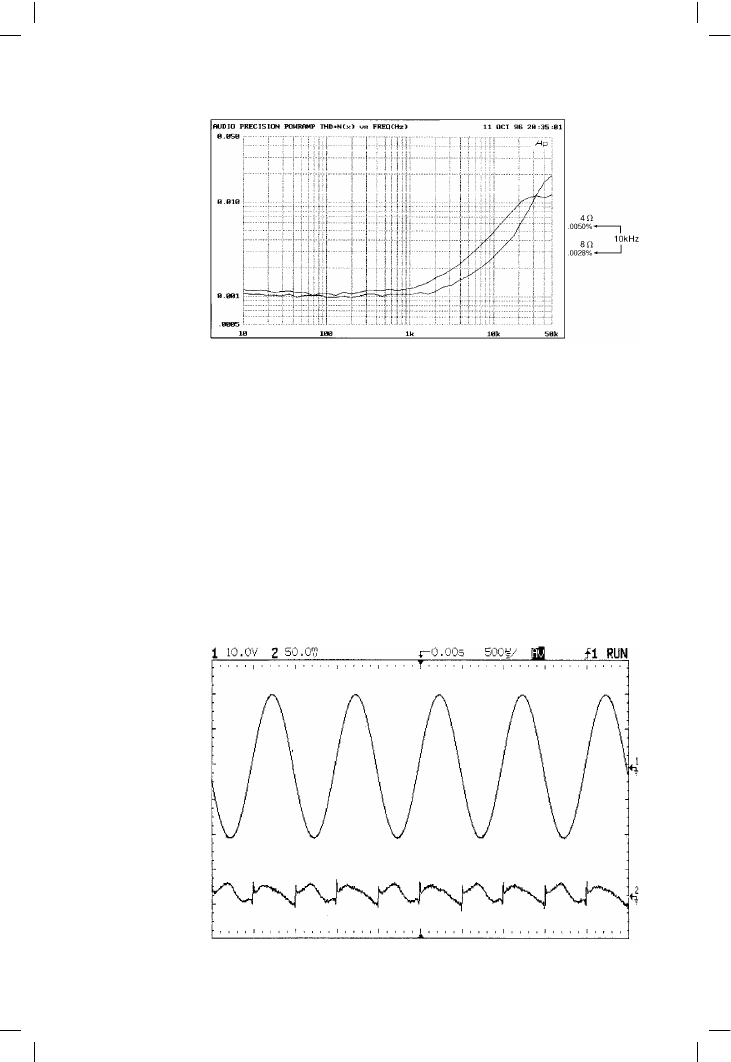
harmonic. In Figure 5.14 the upper trace shows the 4 ! THD is consistently
twice that for 8 !, once it appears above the noise floor.
123

Audio Power Amplifier Design Handbook
I label this Distortion 3a, or Large Signal Non-linearity (LSN), where ‘Large’
refers to currents rather than voltages. Unlike crossover Distortion 3b, the
amount of LSN generated is highly dependent on device characteristics.
The distortion residual is basically third order because of the symmetric and
compressive nature of the output stage gain characteristic, with some
second harmonic because the beta loss is component dependent and not
perfectly symmetrical in the upper and lower output stage halves. Figure
5.15 shows a typical THD residual for Large Signal Non-linearity, driving
50 W into 4 !. The residual is averaged 64 times to reduce noise.
LSN occurs in both emitter-follower (EF) and Complementary Feedback
Pair (CFP) output configurations; this section concentrates on the CFP
version, as shown in Figure 5.5a. Figure 5.16 shows the incremental gain
124
Figure 5.14
Upper trace shows
distortion increase
due to LSN as load
goes from 8 to 4 !.
Blameless amplifier at
25 W/8 !
Figure 5.15
Large Signal Non-
linearity, driving
50 W into 4 ! and
averaged 64 times