ВУЗ: Казахская Национальная Академия Искусств им. Т. Жургенова
Категория: Учебное пособие
Дисциплина: Не указана
Добавлен: 03.02.2019
Просмотров: 17392
Скачиваний: 18
115
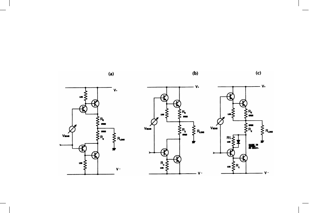
Figure 5.5
CFP circuit and Quasi-
complementary stages
116
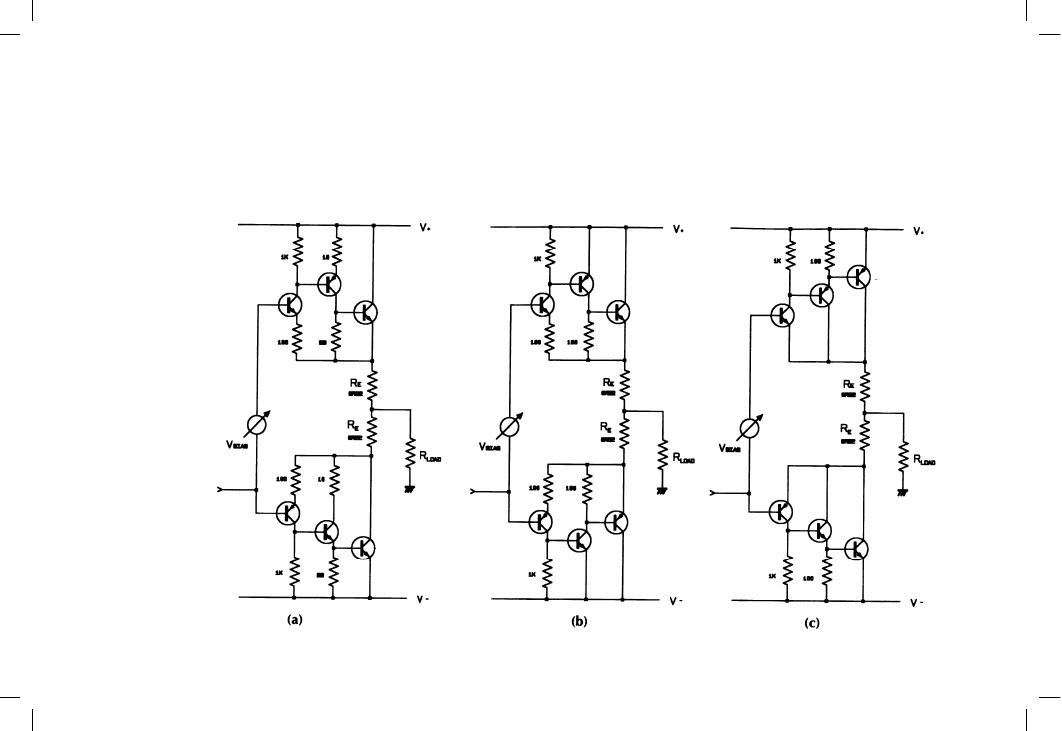
Figure 5.6
Three of the possible
Output-Triple
configurations
The output stage I
(See Table 5.1.) Given also the greater quiescent stability, it is hard to see
why this topology is not more popular.
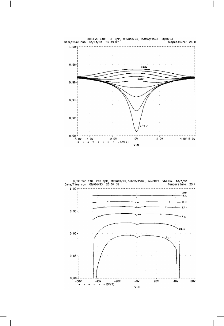
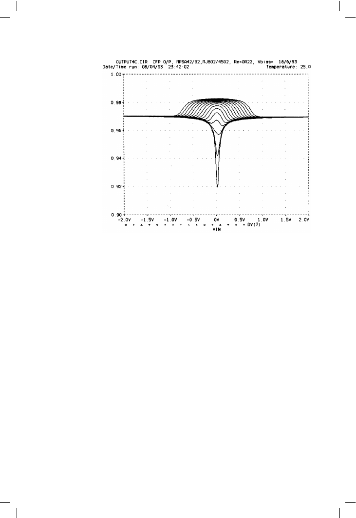
The crossover region is much narrower, at about +/–0.3 V (Figure 5.10).
When under-biased, this shows up on the distortion residual as narrower
spikes than an emitter-follower output gives. The bad effects of gm-
doubling as Vbias increases above optimal (here 1.296 V) can be seen in
the slopes moving outwards from the centre.
117
Table 5.1 Summary of output distortion
Emitter
Follower
CFP
Quasi
Simple
Quasi
Bax
Triple
Type 1
Simple
MOSFET
Quasi
MOSFET
Hybrid
MOSFET
8 !
0.031%
0.014%
0.069%
0.050%
0.13%
0.47%
0.44%
0.052%
Gain:
0.97
0.97
0.97
0.96
0.97
0.83
0.84
0.97
4 !
0.042%
0.030%
0.079%
0.083%
0.60%
0.84%
0.072%
0.072%
Gain:
0.94
0.94
0.94
0.94
0.92
0.72
0.73
0.94
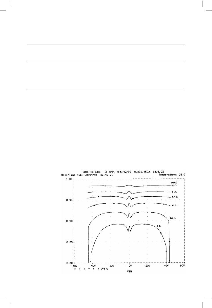
Table 5.1 summarises the SPICE curves for 4 and 8 ! loadings; FET results from Ch.11 are included for
comparison. Each gain plot was subjected to Fourier analysis to calculate THD % results for a +/–40 V input.
Figure 5.7
Emitter-Follower large-
signal gain vs output
Audio Power Amplifier Design Handbook
118
Figure 5.8
EF crossover region
gain deviations,
+/–5 V range
Figure 5.9
Complementary-
Feedback-Pair gain
vs output
The output stage I
119
Figure 5.10
CFP crossover region
+/–2 V, Vbias as a
parameter
Quasi-complementary outputs
Originally, the quasi-complementary configuration
[7]
was virtually man-
datory, as it was a long time before PNP silicon power transistors were
available in anything approaching complements of the NPN versions. The
standard version shown at Figure 5.5b is well known for poor symmetry
around the crossover region, as shown in Figure 5.11. Figure 5.12 zooms in
to show that the crossover region is a kind of unhappy hybrid of the EF and
CFP, as might be expected, and that no setting of Vbias can remove the
sharp edge in the gain plot.
A major improvement to symmetry can be made by using a Baxandall
diode
[8]
, as shown in Figure 5.5c. This stratagem yields gain plots very
similar to those for the true complementary EF at Figures 5.7, 5.8, though
in practice the crossover distortion seems rather higher. When this Quasi-
Baxandall stage is used closed-loop in an amplifier in which Distortions 1
and 2, and 4 to 7 have been properly eliminated, it is capable of much
better performance than is commonly believed; for example, 0.0015%
(1 kHz) and 0.015% (10 kHz) at 100 W is straightforward to obtain from an
amplifier with a moderate NFB factor of about 34 dB at 20 kHz.
The best reason to use the quasi-Baxandall approach today is to save
money on output devices, as PNP power BJTs remain somewhat pricier
than NPNs. Given the tiny cost of a Baxandall diode, and the absolutely
dependable improvement it gives, there seems no reason why anyone
should ever use the standard quasi circuit. My experiments show that the