ВУЗ: Казахская Национальная Академия Искусств им. Т. Жургенова
Категория: Учебное пособие
Дисциплина: Не указана
Добавлен: 03.02.2019
Просмотров: 17396
Скачиваний: 18

The output stage I
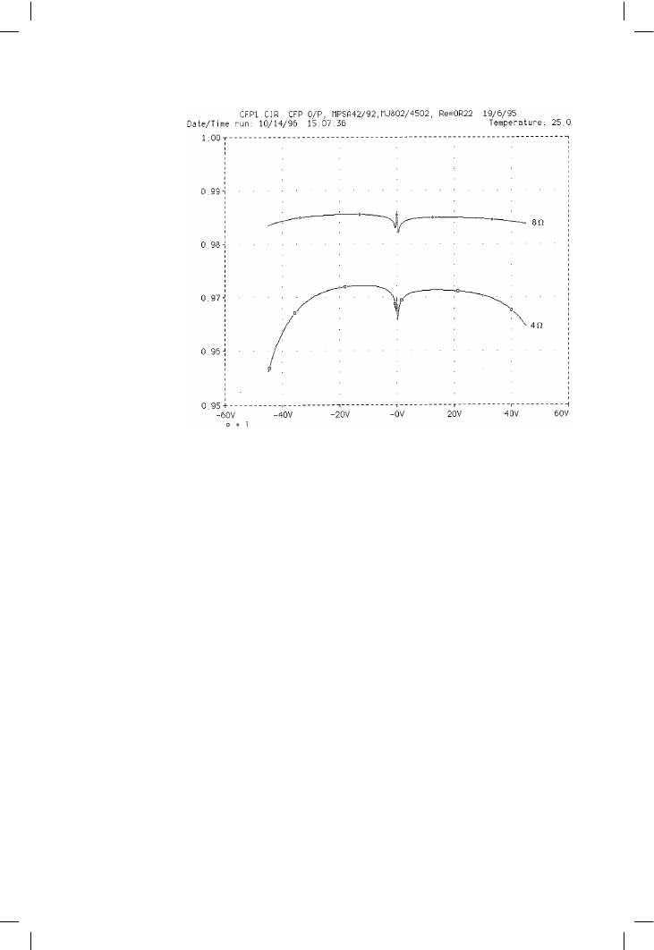
of a simulated CFP output stage for 8 and 4 !; the lower 4 ! trace has
greater downward curvature, i.e. a greater falloff of gain with increasing
current. Note that this falloff is steeper in the negative half, so the THD
generated will contain even as well as odd harmonics. The simulated EF
behaviour is very similar.
As it happens, an 8 ! nominal impedance is a reasonably good match for
standard power BJTs, though 16 ! might be better for minimising LSN if
loudspeaker technology permits. It is coincidental that an 8 ! nominal
impedance corresponds approximately with the heaviest load that can be
driven without LSN appearing, as this value is a legacy from valve
technology. LSN is an extra distortion component laid on top of others, and
usually dominating them in amplitude, so it is obviously simplest to
minimise the 8 ! distortion first. 4 ! effects can then be seen more or less
in isolation when load impedance is reduced.
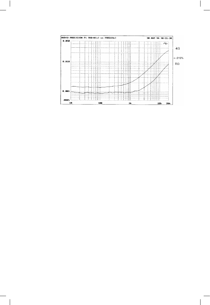
The typical result of 4 ! loading was shown in Figure 5.14, for the modern
MJ15024/25 complementary pair from Motorola. Figure 5.17 shows the
same diagram for one of the oldest silicon complementary pairs, the
2N3055/2955. The 8 ! distortion is similar for the different devices, but the
4 ! THD is 3.0 times worse for the venerable 2N3055/2955. Such is
progress.
Such experiments with different output devices throw useful light on the
Blameless concept – from the various types tried so far it can be said that
125
Figure 5.16
The incremental gain
of a standard CFP
output stage. The
4 ! trace droops
much more as the
gain falls off at
higher currents.
PSpice simulation

Audio Power Amplifier Design Handbook
Blameless performance, whatever the output device type, should not
exceed 0.001% at 1 kHz and 0.006% at 10 kHz, when driving 8 !. The
components existed to build sub-0.001% THD amplifiers in mid-1969, but
not the knowledge.
Low-impedance loads have other implications beyond worse THD. The
requirements for sustained long-term 4 ! operation are severe, demanding
more heatsinking and greater power supply capacity. For economic reasons
the peak/average ratio of music is usually fully exploited, though this can
cause real problems on extended sinewave tests, such as the FTC
40%-power-for-an-hour preconditioning procedure.
The focus of this section is the extra distortion generated in the output stage
itself by increased loading, but there are other ways in which linearity may
be degraded by the higher currents flowing. Of the amplifier distortion
mechanisms (see page 63), Distortions 1, 2, and 8 are unaffected by output
stage current magnitudes. Distortion 4 might be expected to increase, as
increased loading on the output stage is reflected in increased loading on
the VAS. However, both the beta-enhanced EF and buffered-cascode
methods of VAS linearisation deal effectively with sub-8 ! loads, and this
does not seem to be a problem.
When a 4 ! load is driven, the current taken from the power supply is
greater, potentially increasing the rail ripple, which could worsen
Distortion 5. However, if the supply reservoir capacitances have been sized
to permit greater power delivery, their increased capacitance reduces ripple
again, so this effect tends to cancel out. Even if rail ripple doubles, the usual
RC filtering of bias supplies should keep it out of the amplifier, preventing
intrusion via the input pair tail, and so on.
Distortion 6 could worsen as the half-wave currents flowing in the output
circuitry are twice as large, with no counteracting mechanism. Distortion 7,
126
Figure 5.17
4 ! distortion is 3×
greater than 8 ! for
2N3055/2955
output devices.
Compare Figure
5.14

The output stage I
The load-invariant concept
In an ideal amplifier the extra LSN distortion component would not exist.
Such an amplifier would give no more distortion into 4 ! than 8, and could
be called ‘Load-Invariant to 4 !’. The minimum load qualification is
required because it will be seen that the lower the impedance, the greater
the difficulties in aspiring to Load-Invariance. I assume that we start out
with an amplifier that is Blameless at 8 !; it would be logical but quite
pointless to apply the term ‘Load-Invariant’ to an ill-conceived amplifier
delivering 1% THD into both 8 and 4 !.
The LSN mechanism
When the load impedance is reduced, the voltage conditions are
essentially unchanged. LSN is therefore clearly a current-domain effect, a
function of the magnitude of the signal currents flowing in drivers and
output devices.
A 4 ! load doubles the output device currents, but this does not in itself
generate significant extra distortion. The crucial factor appears to be that
the current drawn from the drivers by the output device bases more than
doubles, due to beta falloff in the output devices as collector current
increases. It is this extra increase of current that causes almost all the
additional distortion. The exact details of this have not been completely
clarified, but it seems that this ‘extra current’ due to beta falloff varies very
non-linearly with output voltage, and combines with driver non-linearity to
reinforce it rather than cancel. Beta-droop is ultimately due to high-level
injection effects, which are in the province of semiconductor physics rather
than amplifier design. Such effects vary greatly with device type, so when
output transistors are selected, the likely performance with loads below 8 !
must be considered.
There is good simulator evidence that LSN is entirely due to beta-droop
causing extra current to be drawn from the drivers. To summarise:
!
Simulated output stages with output devices modified to have no beta-
droop (by increasing SPICE model parameter IKF) do not show LSN. It
127
if present, will be worse due to the increased load currents flowing in the
output stage wiring resistances.
Of those mechanisms above, Distortion 4 is inherent in the circuit
configuration (though easily reducible below the threshold of measure-
ment) while 5, 6, and 7 are topological, in that they depend on the spatial
and geometrical relationships of components and wiring. The latter three
distortions can therefore be completely eliminated in both theory and
practice. This leaves only the LSN component, otherwise known as
Distortion 3a, to deal with.

Audio Power Amplifier Design Handbook
appears to be specifically that extra current taken due to beta-droop
causes the extra non-linearity.
!
Simulated output devices driven with zero-impedance voltage sources
instead of the usual transistor drivers exhibit no LSN. This shows that
LSN does not occur in the outputs themselves, and so it must be
happening in the driver transistors.
!
Output stage distortion can be treated as an error voltage between
input and output. The double emitter-follower (EF) stage error is
therefore: driver Vbe + output Vbe + Re drop. A simulated EF output
stage with the usual drivers shows that it is primarily non-linearity
increases in the driver Vbe rather than in the output Vbe, as load
resistance is reduced. The voltage drop across the emitter resistors Re
is essentially linear.
The knowledge that beta-droop caused by increased output device Ic is at
the root of the problem leads to some solutions. Firstly, the per-device Ic
can be reduced by using parallel output devices. Alternatively Ic can be left
unchanged and output device types selected for those with the least beta-
droop.
Doubled output devices
LSN can be effectively reduced by doubling the output devices, when this
is quite unnecessary for handling the rated power output. The falloff of beta
depends on collector current, and if two output devices are connected in
parallel, the collector current divides in two between them. Beta-droop is
much reduced.
From the above evidence, I predicted that this doubling ought to reduce
LSN – and when measured, indeed it does. Such reality checks must never
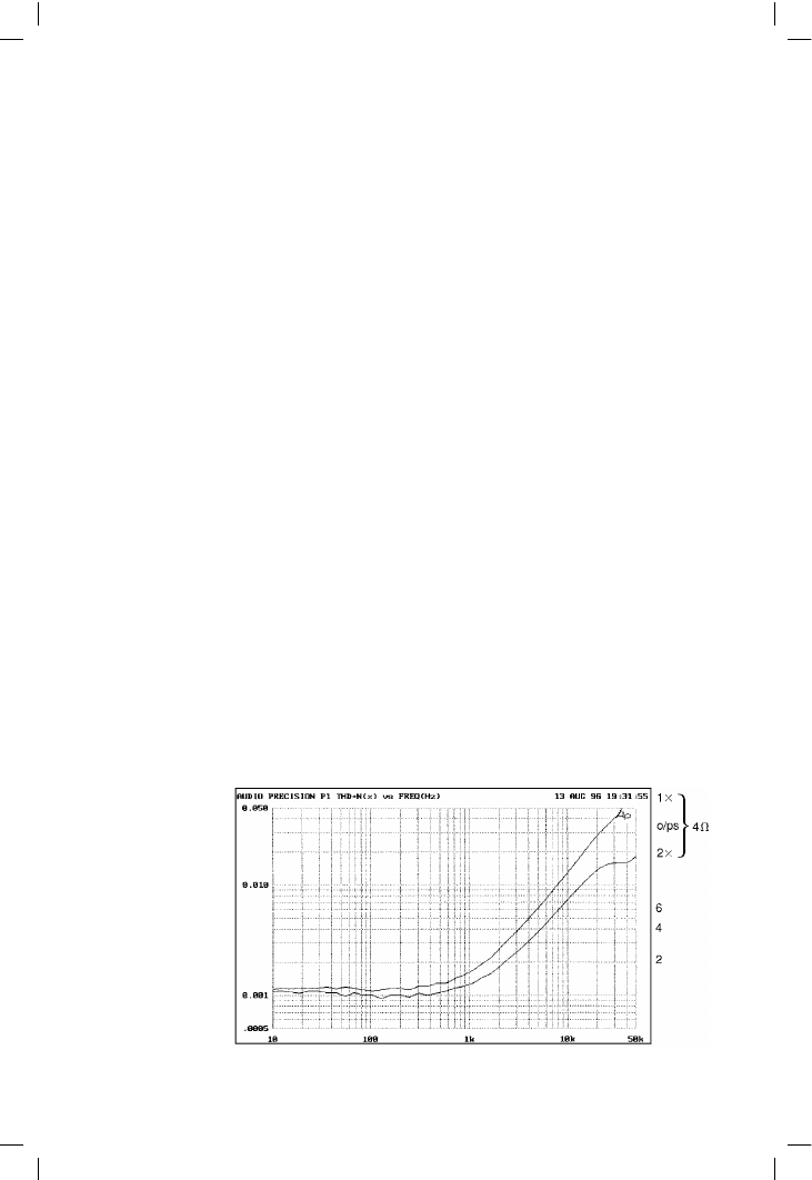
be omitted when using circuit simulators. Figure 5.18 compares the 4 !
THD at 60 W for single and double output devices, showing that doubling
128
Figure 5.18
4 ! distortion is
reduced by 1.9×
upon doubling
standard
(MJ15024/15025)
output transistors.
30 W/8 !

The output stage I
reduces distortion by about 1.9 times, which is a worthwhile improvement.
The output transistors used for this test were modern devices, the Motorola
MJ15024/15025. The much older 2N3055/2955 complementary pair give
a similar halving of LSN when their number is doubled, though the initial
distortion is three times higher into 4 !. 2N3055 specimens with an H
suffix show markedly worse linearity than those without.
No explicit current-sharing components were added when doubling the
devices, and this lack seemed to have no effect on LSN reduction. There
was no evidence of current hogging, and it appears that the circuit cabling
resistances alone were sufficent to prevent this.
Doubling the number of power devices naturally increases the power
output capability, though if this is exploited LSN will tend to rise again, and
you are back where you started. Opting for increased power output will
also make it necessary to uprate the power supply, heatsinks, and so on.
The essence of this technique is to use parallel devices to reduce distortion
long before power handling alone compels you to do so.
Better output devices
The 2SC3281 2SA1302 complementary pair are plastic TO3P devices with
a reputation in the hi-fi industry for being ‘more linear’ than the general run
of transistors. Vague claims of this sort arouse the deepest of suspicions;
compare the many assertions of superior linearity for power FETs, which is
the exact opposite of reality. However, in this case the core of truth is that
2SC3281 and 2SA1302 show much less beta-droop than average power
transistors. These devices were introduced by Toshiba; Motorola versions
are MJL3281A, MJL1302A, also in TO3P package. Figure 5.19 shows beta-
droop, for the various devices discussed here, and it is clear that more
droop means more LSN.
The 3281/1302 pair are clearly in a different class from conventional
transistors, as they maintain beta much more effectively when collector
current increases. There seems to be no special name for this class of BJTs,
so I have called them ‘sustained-beta’ devices here.
The THD into 4 and 8 ! for single 3281/1302 devices is shown in Figure
5.20. Distortion is reduced by about 1.4 times compared with the standard
devices of Figure 5.14, over the range 2–8 kHz. Several pairs of 3281/1302
were tested and the 4 ! improvement is consistent and repeatable.
The obvious next step is to combine these two techniques by using doubled
sustained-beta devices. The doubled-device results are shown in Figure
5.21 where the distortion at 80 W/4 ! (15 kHz) is reduced from 0.009% in
Figure 5.20 to 0.0045%; in other words, halved. The 8 and 4 ! traces are
now very close together, the 4 ! THD being only 1.2 times higher than in
the 8 ! case.
129