ВУЗ: Казахская Национальная Академия Искусств им. Т. Жургенова
Категория: Учебное пособие
Дисциплина: Не указана
Добавлен: 03.02.2019
Просмотров: 17398
Скачиваний: 18
Audio Power Amplifier Design Handbook
130
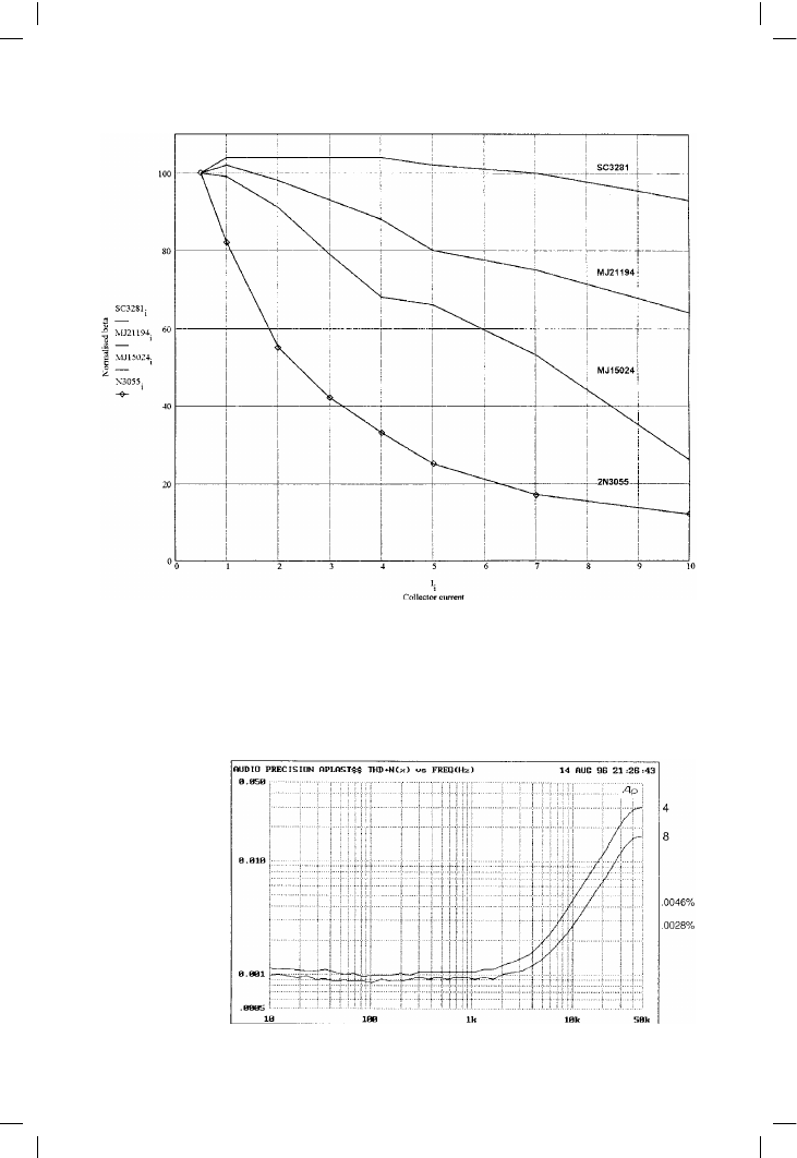
Figure 5.19
Power transistor beta falls as collector current increases. Beta is normalised to 100 at 0.5 A (from
manufacturers’ data sheets)
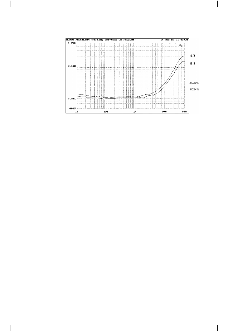
Figure 5.20
THD at 40 W/8 !
and 80 W/4 ! with
single 3281/1302
devices
The output stage I
There are other devices showing less beta-droop than standard. In a very
quick survey I unearthed the MJ21193, MJ21194 pair (TO3 package) and
the MJL21193, MJL21194 pair (TO3P package), both from Motorola. These
devices show beta-maintenance intermediate between the ‘super’
3281/1302 and ‘ordinary’ MJ15024/25, so it seemed likely that they would
give less LSN than ordinary power devices, but more than the 3281/1302.
This prediction was tested and duly fulfilled.
It could be argued that multiplying output transistors is an expensive way to
solve a linearity problem. To give this perspective, in a typical stereo power
amplifier the total cost including heatsink, metal work and mains
transformer will only increase by about 5% when the output devices are
doubled.
Feedforward diodes
The first technique I tried to reduce LSN was the addition of power diodes
across OR22 output emitter resistors. The improvement was only sig-
nificant for high power into sub-3 ! loading, and was of rather doubtful
utility for hi-fi. Feedforward diodes treat the symptoms (by attempting
distortion cancellation) rather than the root cause, so it is not surprising this
method is of limited effectiveness; see Figure 5.25.
It is my current practice to set the output emitter resistors Re at 0.1 !, rather
than the more common OR22. This change both improves voltage-swing
efficiency and reduces the extra distortion generated if the amplifier is
erroneously biased into Class AB. As a result even low-impedance loads
give a relatively small voltage drop across Re, which is insufficient to turn
on a silicon power diode at realistic output levels.
Schottky diodes have a lower forward voltage drop and might be useful
here. Tests with 50 A diodes have been made but have so far not been
131
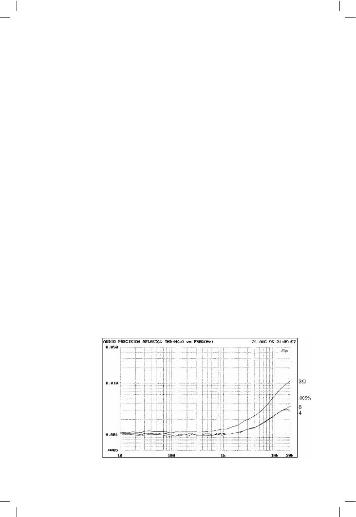
Figure 5.21
THD at 40 W/8 !
and 80 W/4 ! with
doubled
3281/1302 output
transistors. 4 ! THD
has been halved
compared with
Figure 5.12
Audio Power Amplifier Design Handbook
encouraging in the distortion reduction achieved. Suitable Schottky diodes
cost at least as much as an output transistor, and two will be needed.
Trouble with triples
In electronics, as in many fields, there is often a choice between applying
brawn (in this case multiple power devices) or brains to solve a given
problem. The ‘brains’ option here would be a clever circuit configuration
that reduced LSN without replication of expensive power silicon, and the
obvious place to look is the output-triple approach. Note ‘output triples’ here
refers to pre-driver, driver, and output device all in one local NFB loop, rather
than three identical output devices in parallel, which I would call ‘tripled
outputs’. Getting the nomenclature right is a bit of a problem.
In simulation, output-triple configurations do reduce the gain-droop that
causes LSN. There are many different ways to configure output triples, and
they vary in their linearity and immunity to LSN. The true difficulty with this
approach is that three transistors in a tight local loop are very prone to
parasitic and local oscillations. This tendency is exacerbated by reducing
the load impedances, presumably because the higher collector currents
lead to increased device transconductance. This sort of instability can be
very hard to deal with, and in some configurations appears almost
insoluble. At present this approach has not been studied further.
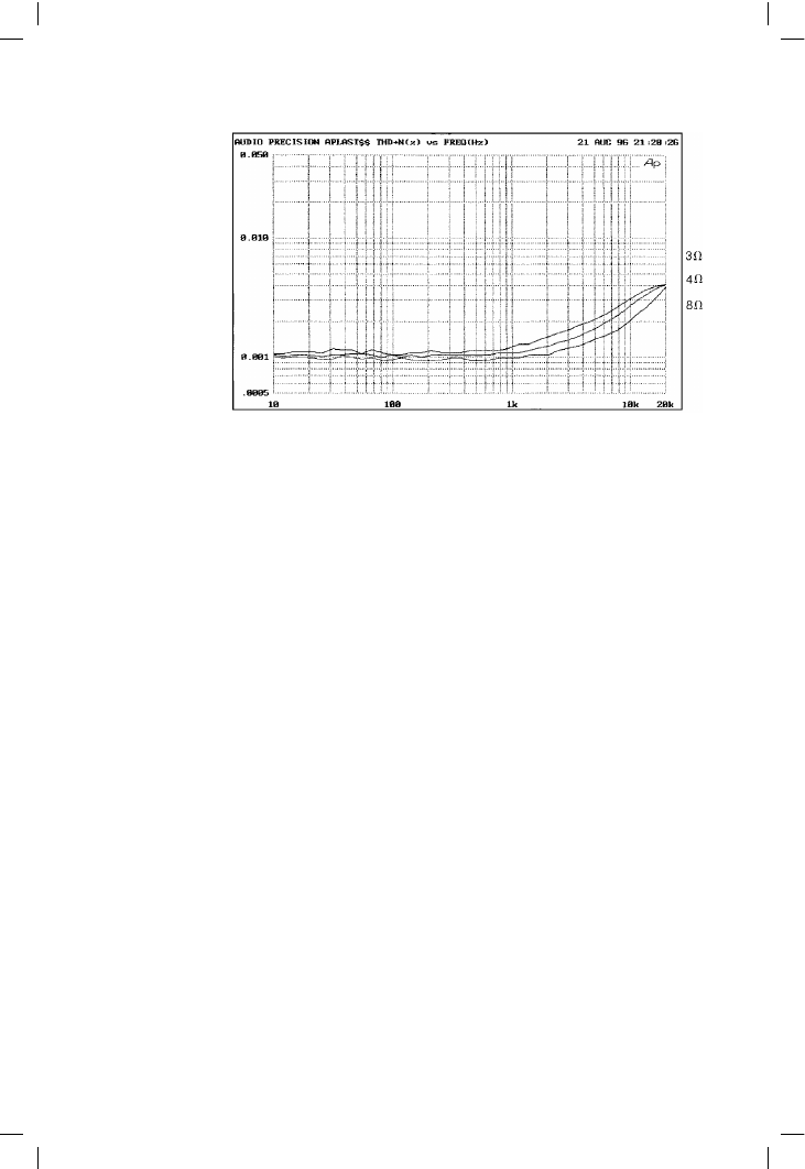
Loads below 4 !
So far I have concentrated on 4 ! loads; loudspeaker impedances often
sink lower than this, so further tests were done at 3 !. One pair of
3281/1302 devices will give 50 W into 3 ! for THD of 0.006% (10 kHz),
see Figure 5.22. Two pairs of 3281/1302 reduce the distortion to 0.003%
(10 kHz) as in Figure 5.23. This is an excellent result for such simple
circuitry, and may well be a record for 3 ! linearity.
132
Figure 5.22
Distortion for 3, 4 and
8 ! loads, single
3281/1302 devices.
20 W/8 !,
40 W/4 ! and
60 W/3 !
The output stage I
It appears that whatever the device type, doubling the outputs halves the
THD percentage for 4 ! loading. This principle can be extended to 2 !
operation, but tripled devices are required for sustained operation at
significant powers. The resistive losses will be serious, so 2 ! power output
may be little greater than that into 4 !.
Better 8 ! performance
It was not expected that the sustained-beta devices would also show lower
crossover distortion at 8 !, but they do, and the effect is once more
repeatable. It may be that whatever improves the beta characteristic also
somewhat alters the turn-on law so that crossover distortion is reduced;
alternatively traces of LSN, not visible in the THD residual, may have been
eliminated. The latter is probably the more likely explanation.
The plot in Figure 5.23 shows the improvement over the MJ15024/25
pair; compare the 8 ! line in Figure 5.14. The 8 ! THD at 10 kHz is
reduced from 0.003% to 0.002%, and with correct bias adjustment, the
crossover artefacts are invisible on the 1 kHz THD residual. Crossover
artefacts are only just visible in the 4 ! case, and to get a feel for the
distortion being produced, and to set the bias optimally, it is necessary
to test at 5 kHz into 4 !.
A practical load-invariant design
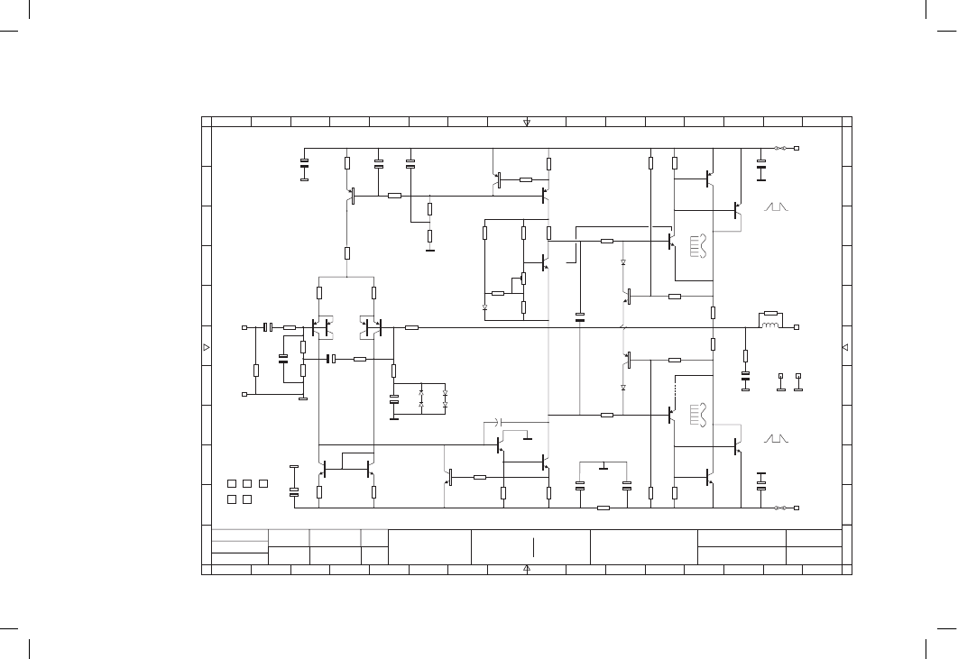
Figure 5.24 is the circuit of a practical Load-Invariant amplifier designed for
8 ! nominal loads with 4 ! impedance dips; not for speakers that start out
at 4 ! nominal and plummet from there. The distortion performance is
shown in Figures 5.21 and 5.22 for various fitments of output device. The
supply voltage can be from +/–20 to +/–40 V; checking power capability
for a given output device fit must be left to the constructor.
133
Figure 5.23
Distortion for 3, 4 and
8 ! load, double
3281/1302 devices.
Power as Figure 5.22
1
1
A
E
C
G
J
B
F
I
D
H
K
7
7
4
4
10
10
2
2
8
8
5
5
11
11
3
3
9
9
6
6
12
12
Approved:
Issue:
Fix1
Input
signal
Input
ground
P1
R1
100k
C1
47/25
C3
47/25
C2
1n
0VA
0VA
0VA
0VA
0VA
1
1
1
2
2
2
2
1
3
3
3
1
1
1
1
3
2
2
2
C7
100n
Q3
MPSA06
Q9
MPSA06
Q10
MPSA06
Q8
MJE340
Q7
MPSA56
Q6
MPSA56
Q6
MPSA56
R6
6R
R6
6R
Q4
MPSA06
R2
10R
R16
2k2
R9
100R
R9
100R
R29
100R
R28
100R
R23
16R
R18
68R
R17
2k2
R21
680R
R22
270R
R20
270R
PR1
1k
R19
270R
Q8 & Q14 mounted
on top of each other
C9
100p
R25
2k2
R31
22k
R30
22k
R26
10R
R27
10R
R3
1k1
R5
100R
R11
2k2
R10
100R
R13
10k
R14
10k
R7
100R
R15
110R
C8
1000/10
C10
1000/35
C4
47/25
C5
47/25
C11
100n
D1
1N414B
1N414B
D3
D2
1N414B
1N414B
D3
+
+
+
+
R4
1k1
MPSA56
Q1
MPSA56
Q2
Q101
2SB737
Q102
2SB737
Fit either
MPSA56 or 2SB737
3
3
1
2
1
3
3
2
2
2
1
+
+
Fix4
Fix2
Fix5
Fix3
2
041196
Material:
Scale:
Key:
The Signal Transfer Co. owns the
copyright of this drawing, which may
not be copied, reproduced or
disclosed, in part or in whole, to a
third party without written permission.
Date:
Finish:
Checked:
DOUGLAS SELF
Drawn by:
GARETH CONNOR
1
1
1
1
1
2
3
3
3
3
3
1
2
1
3
Q11
MPSA06
2
1
1
2
2
Q13
MPSA56
Q12
MPSA06
1N4148
D7
1N4148
D6
3
3
3
3
C12
47/25
+
1N4148
D5
+
–
0VA
0VA
C6
100n
R12
2k2
A
E
C
G
J
B
F
I
D
H
K
14
14
15
15
13
13
16
16
Title:
Drawing No.
SHEET 1 OF 1 SHEETS
LOAD INVARIANT POWER AMP
0VA
0VA
0VA
0VA
0VA
Clip-TSC506
Clip4
Clip-TSC506
Clip4
Clip2
Clip1
C
lip
-S
W
25
C
lip
-S
W
25
HS2
HS1
LK2
LK1
SW38
SW38
R35
270R
270R
R34
R33
100R
R32
100R
C14
220/63
C13
220/63
L1
P6
P6
P6
FH2
1A
FH1
1A
-V
Power
-V
Power
Output
signal
Power
ground
P7
Output
ground
P4
+
+
2
2
3
3
Q17
2SC3281
Q16
2SA1302
1
1
2
2
3
3
Q19
2SC3281
Q18
2SA1302
1
1
1
1
2
2
Q15
MJE350
R39
10R
R3
10R
C15
100n
R37
0R1
R36
0R1
Q14
MJE340
134
Figure 5.24
Circuit diagram of
the Load-Invariant
power amplifier