ВУЗ: Казахская Национальная Академия Искусств им. Т. Жургенова
Категория: Учебное пособие
Дисциплина: Не указана
Добавлен: 03.02.2019
Просмотров: 17403
Скачиваний: 18
Audio Power Amplifier Design Handbook
The Vbe-Ic characteristic of a bipolar transistor is initially exponential,
blending into linear as the internal emitter resistance re comes to dominate
the transconductance. The usual Class-B stage puts two of these curves
back-to-back, and Peter Blomley has shown
[12]
that these curves are non-
conjugate, i.e. there is no way they can be shuffled about so they will sum
to a completely linear transfer characteristic, whatever the offset between
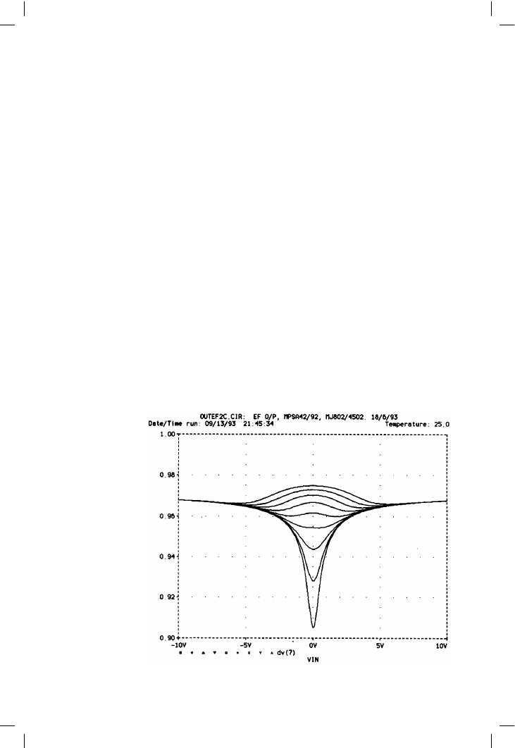
them imposed by the bias voltage. This can be demonstrated quickly and
easily by SPICE simulation; see Figure 5.31. There is at first sight not much
you can do except maintain the bias voltage, and hence quiescent current,
at some optimal level for minimum gain deviation at crossover; quiescent-
current control is a complex subject that could fill a big book in itself, and
is considered in Chapter 12.
It should be said that the crossover distortion levels generated in a
Blameless amplifier can be very low up to around 1 kHz, being barely
visible in residual noise and only measurable with a spectrum-analyser. As
an instructive example, if a Blameless closed-loop Class-B amplifier is
driven through a TL072 unity-gain buffer the added noise from this op-amp
will usually submerge the 1 kHz crossover artefacts into the noise floor, at
least as judged by the eye on the oscilloscope. (It is most important to note
that Distortions 4, 5, 6 and 7 create disturbances of the THD residual at the
zero-crossing point that can be easily mistaken for crossover distortion, but
the actual mechanisms are quite different). However, the crossover
distortion becomes obvious as the frequency increases, and the high-order
harmonics benefit less from NFB.
140
Figure 5.31
Gain/output voltage
plot for an EF output
shows how non-
conjugate transistor
characteristics at the
crossover region
cannot be blended into
a flat line at any bias
voltage setting. Bias
varies 2.75 to 2.95 V
in 25 mV steps, from
too little to too much
quiescent
The output stage I
It will be seen later that in a Blameless amplifier driving 8 ! the overall
linearity is dominated by crossover distortion, even with a well-designed
and optimally biased output stage. There is an obvious incentive to
minimise this distortion mechanism, but there seems no obvious way to
reduce crossover gain deviations by tinkering with any of the relatively
conventional stages considered so far.
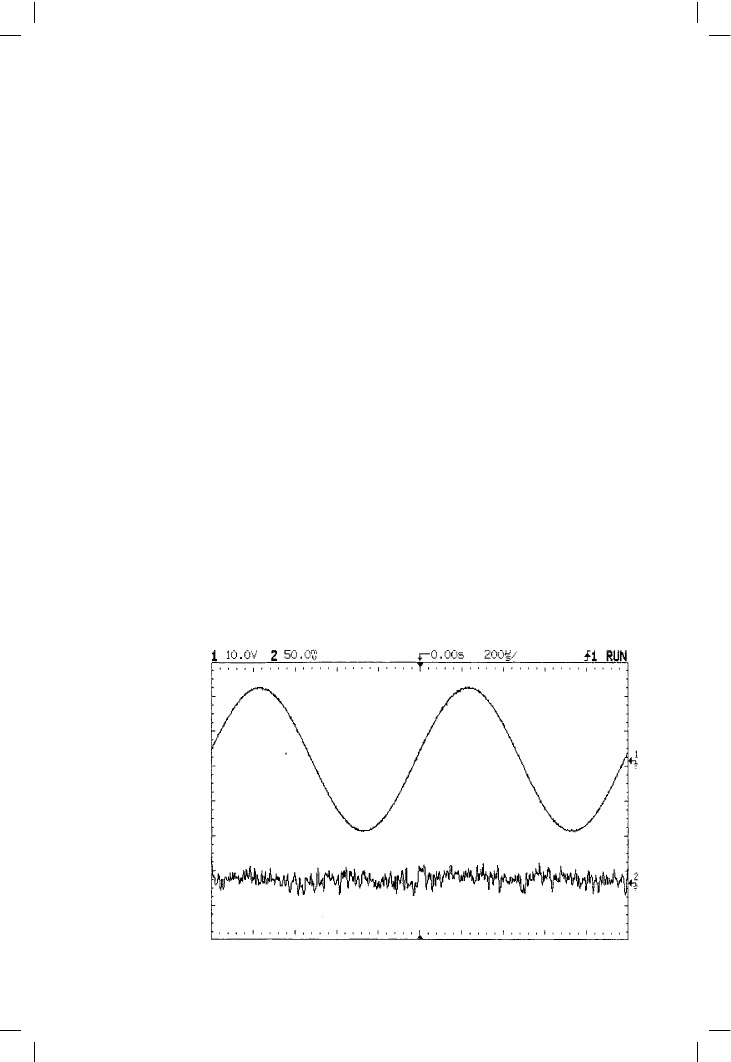
Figure 5.32 shows the signal waveform and THD residual from a Blameless
power amplifier with optimal Class-B bias. Output power was 25 W into
8 !, or 50 W into 4 ! (i.e. the same output voltage) as appropriate, for all
the residuals shown here. The figure is a record of a single sweep so the
residual appears to be almost totally random noise; without the visual
averaging that occurs when we look at an oscilloscope the crossover
artefacts are much less visible than in real time.
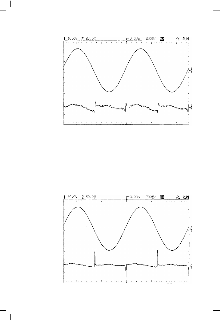
In Figure 5.33 64 times averaging is applied, and the disturbances around
crossover become very clear. There is also revealed a low-order compo-
nent at roughly 0.0004%, which is probably due to very small amounts
of Distortion 6 that were not visible when the amplifier layout was
optimised.
Figure 5.34 shows Class-B slightly underbiased to generate crossover
distortion. The crossover spikes are very sharp, so their height in the
residual depends strongly on measurement bandwidth. Their presence
warns immediately of underbiasing and avoidable crossover distortion.
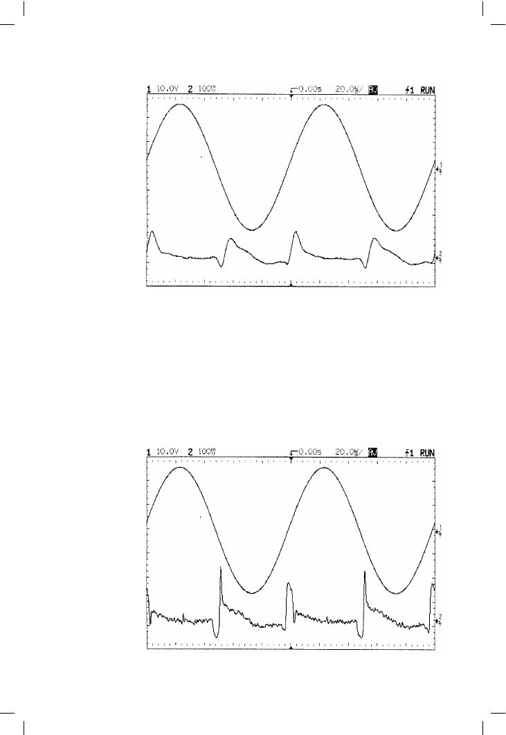
In Figure 5.35 an optimally biased amplifier is tested at 10 kHz. The THD
increases to approx. 0.004%, as the amount of global negative feedback
is 20 dB less than at 1 kHz. The timebase is faster so crossover events
141
Figure 5.32
The THD residual
from an optimally
biased Blameless
power amplifier at
1 kHz, 25 W/8 ! is
essentially white
noise. There is some
evidence of artefacts
at the crossover
point, but they are
not measurable. THD
0.00097%, 80 kHz
bandwidth
Audio Power Amplifier Design Handbook
appear wider than in Figure 5.34. The THD level is now higher and
above the noise so the residual is averaged 8 times only. The measure-
ment bandwidth is still 80 kHz, so harmonics above the eighth are now
lost. This is illustrated in Figure 5.36, which is Figure 5.35 rerun with a
500 kHz bandwidth. The distortion products now look much more
jagged.
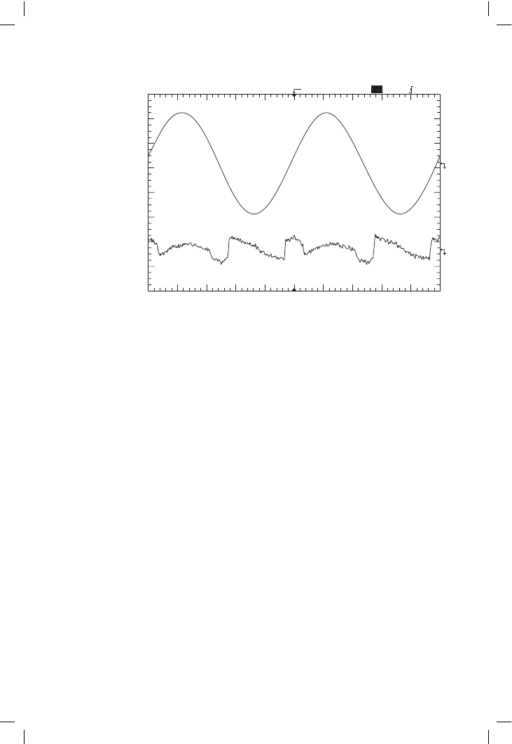
Figure 5.37 shows the gain-step distortion introduced by Class-AB. The
undesirable edges in the residual are no longer in close pairs that partially
142
Figure 5.33
Averaging Figure 5.2
residual 64 times
reduces the noise by
18 dB, and crossover
discontinuities are
now obvious. The
residual has been
scaled up by 2.5
times from Figure 5.2
for greater clarity
Figure 5.34
The results of mild
underbias in Class-B
The output stage I
cancel, but are spread apart on either side of the zero crossing. No
averaging is used here as the THD is higher. See page 275 for more on
Class-AB distortion.
It is commonplace in Audio to discover that a problem like crossover
distortion has been written about and agonised over for decades, but the
amount of technical investigation that has been done (or at any rate
published) is disappointingly small. I had to do some basic investigations
myself.
143
Figure 5.35
An optimally biased
Blameless power
amplifier at 10 kHz.
THD approx.
0.004%, bandwidth
80 kHz. Averaged 8
times
Figure 5.36
As Figure 5.6, but in
500 kHz bandwidth.
The distortion
products look quite
different
1
2
10.0V
20.0
0.00s
200
1 RUN
/
m
v
"
s
AV
1
2
Audio Power Amplifier Design Handbook
I first looked to see if crossover distortion really did increase with
decreasing output level in a Blameless amplifier; to attempt its study with
an amplifier contaminated with any of the avoidable distortion mecha-
nisms is completely pointless. One problem is that a Blameless amplifier
has such a low level of distortion at 1 kHz (0.001% or less) that the
crossover artefacts are barely visible in circuit noise, even if low-noise
techniques are used. The measured percentage level of the noise-plus-
distortion residual is bound to rise with falling output, because the noise
voltage remains constant; this is the lowest line in Figure 5.38. To
circumvent this, the amplifier was deliberately underbiased by varying
amounts to generate ample crossover spikes, on the assumption that any
correctly adjusted amplifier should be less barbarous than this.
The answer from Figure 5.38 is that the THD percentage does increase as
level falls, but relatively slowly. Both EF and CFP output stages give similar
diagrams to Figure 5.38, and whatever the degree of underbias, THD
increases by about 1.6 times as the output voltage is halved. In other words,
reducing the output power from 25 W to 250 mW, which is pretty drastic,
only increases THD % by six times, and so it is clear that the absolute (as
opposed to percentage) THD level in fact falls slowly with amplitude, and
therefore probably remains imperceptible. This is something of a relief; but
crossover distortion remains a bad thing to have.
Distortion versus level was also investigated at high frequencies, i.e. above
1 kHz where there is more THD to measure, and optimal biasing can be
used. Figure 5.39 shows the variation of THD with level for the EF stage at
a selection of frequencies; Figure 5.40 shows the same for the CFP. Neither
shows a significant rise in percentage THD with falling level, though it is
144
Figure 5.37
The gm-doubling
distortion introduced
by Class-AB. The
edges in the residual
are larger and no
longer at the zero
crossing, but
displaced either side
of it