ВУЗ: Казахская Национальная Академия Искусств им. Т. Жургенова
Категория: Учебное пособие
Дисциплина: Не указана
Добавлен: 03.02.2019
Просмотров: 17405
Скачиваний: 18

The output stage I
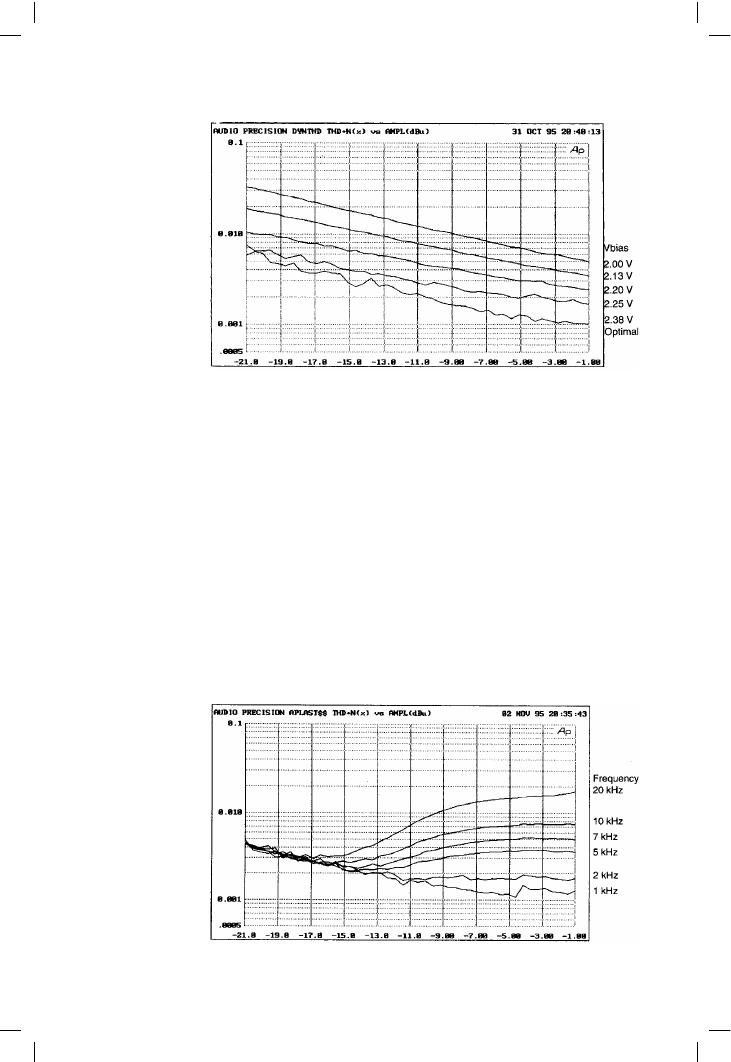
noticeable that the EF gives a good deal less distortion at lower power
levels around 1 W. This is an unexpected observation, and possibly a new
one.
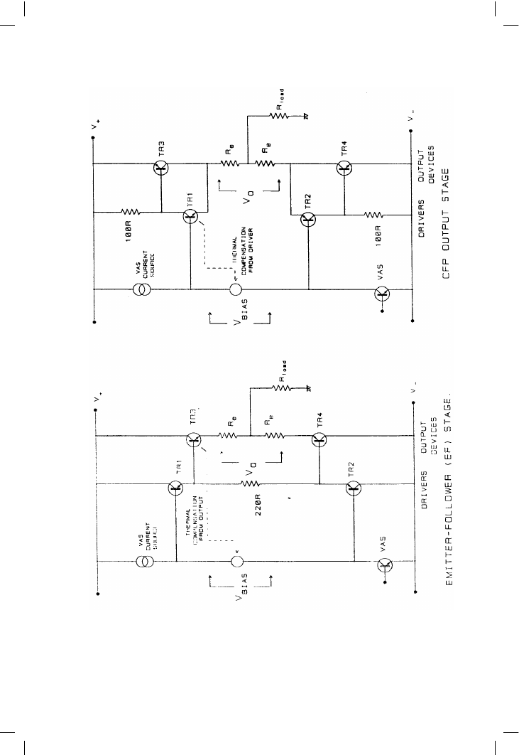
To further get the measure of the problem, Figure 5.41 shows how HF
distortion is greatly reduced by increasing the load resistance, providing
further confirmation that almost all the 8 ! distortion originates as
crossover in the output stage.
Crossover distortion, unlike some more benign kinds of signal-warping, is
unanimously agreed to be something any amplifier could well do
without. The amount of crossover distortion produced depends strongly
on optimal quiescent adjustment, so the thermal compensation used to
stabilise this against changes in temperature and power dissipation must
be accurate. This section deals with the crossover region and its
145
Figure 5.38
Showing how
crossover distortion
rises slowly as output
power is reduced
from 25 W to
250 mW (8 !) for
optimal bias and
increasingly severe
underbias (upper
lines). This is an EF
type output stage.
Measurement
bandwidth 22 kHz
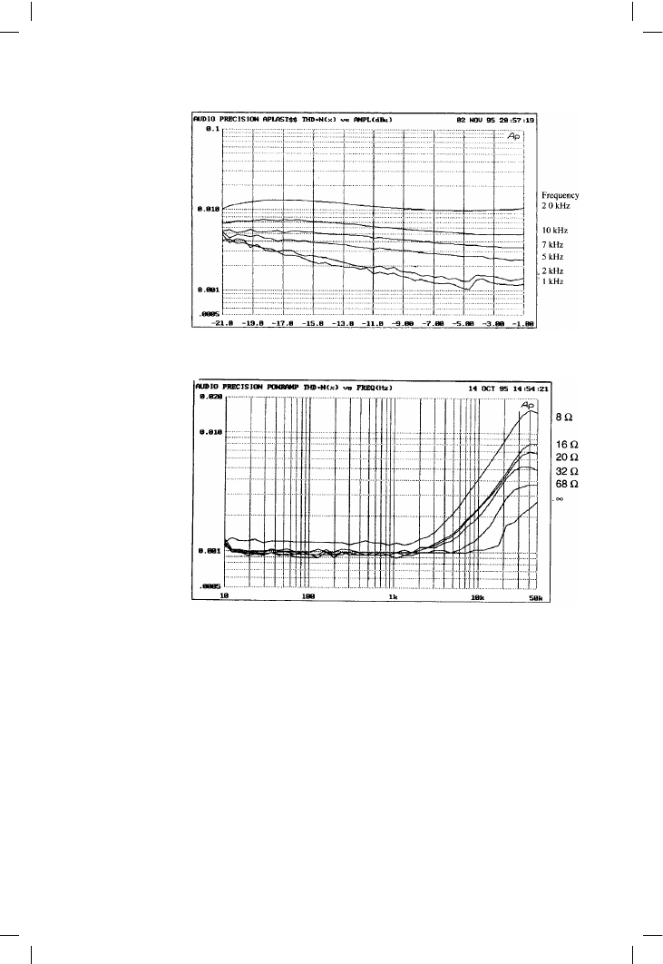
Figure 5.39
Variation of crossover
distortion with output
level for higher
frequencies.
Optimally biased EF
output stage.
Bandwidth 80 kHz

Audio Power Amplifier Design Handbook
quiescent conditions, and the specific issues of the effectiveness of the
thermal compensation for temperature effects is dealt with in detail in
Chapter 12.
Output stage quiescent conditions
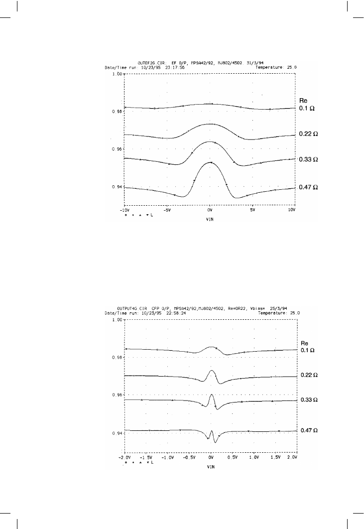
Figure 5.42 shows the two most common types of output stage: the
Emitter-Follower (EF) and the Complementary-Feedback-Pair (CFP) config-
urations. The manifold types of output stage based on triples will have to
be set aside for the moment. The two circuits shown have few
components, and there are equally few variables to explore in attempting
to reduce crossover distortion.
146
Figure 5.40
Variation of distortion
with level for higher
frequencies.
Optimally biased
CFP output stage.
Bandwidth 80 kHz
Figure 5.41
How crossover
distortion is reduced
with increasing load
resistance. 20 W into
8 !, 80 kHz
bandwidth

147
Figure
5.42
The
two
most
popular
kinds
of
output
stage:
the
emitter-follower
(EF)
and
Complementar
y
Feedback
Pair
(CFP)
Vbias
and
Vq
are
identified

Audio Power Amplifier Design Handbook
To get the terminology straight: here, as in my previous writings, Vbias
refers to the voltage set up across the driver bases by the Vbe-multiplier bias
generator, and is in the range 1–3 V for Class-B operation. Vq is the
quiescent voltage across the two emitter resistors (hereafter Re) alone, and
is between 5 and 50 mV, depending on the configuration chosen.
Quiescent current lq refers only to that flowing in the output devices, and
does not include driver standing currents.
I have already shown that the two most common output configurations are
quite different in behaviour, with the CFP being superior on most criteria.
Table 5.2 shows that crossover gain variation for the EF stage is smoother,
(being some 20 times wider) but of four times higher amplitude than for the
CFP version. It is not immediately obvious from this which stage will
generate the least HF THD, bearing in mind that the NFB factor falls with
frequency.
Table 5.2 also emphasises that a little-known drawback of the EF version is
that its quiescent dissipation may be far from negligible.
An experiment on crossover distortion
Looking hard at the two output stage circuit diagrams, intuition suggests
that the value of emitter resistor Re is worth experimenting with. Since
these two resistors are placed between the output devices, and alternately
pass the full load current, it seems possible that their value could be critical
in mediating the handover of output control from one device to the other.
Re was therefore stepped from 0.1 to 0.47 !, which covers the practical
range. Vbias was reoptimised at each step, though the changes were very
small, especially for the CFP version.
148
Table 5.2
Emitter-follower
CFP
Vbias
2.930 V
1.297 V
Vq
50 mV
5 mV
Iq
114 mA
11 mA
Pq (per o/p device)
4.6 W
0.44 W
Average gain
0.968
0.971
Peak gain deviation from average
0.48%
0.13%
Crossover width*
+/–12 V
+/–0.6 V
(For Re = 0R22, 8 ! load, and +/–40 V supply rails)
* Crossover-width is the central region of the output voltage range over which crossover
effects are significant; I have rather arbitrarily defined it as the +/– output range over
which the incremental gain curves diverge by more than 0.0005 when Vbias is altered
around the optimum value. This is evaluated here for an 8 ! load only.

The output stage I
Figure 5.43 shows the resulting gain variations in the crossover region for
the EF stage, while Figure 5.44 shows the same for the CFP configuration.
Table 5.3 summarises some numerical results for the EF stage, and Table 5.4
for the CFP.
There are some obvious features; firstly Re is clearly not critical in value as
the gain changes in the crossover region are relatively minor. Reducing the
149
Figure 5.43
Output linearity of the
EF output stage for
emitter-resistance Re
between 0.1 and
0.47 !
Figure 5.44
Output linearity of the
CFP output stage for
emitter-resistance Re
between 0.1 and
0.47 !