ВУЗ: Казахская Национальная Академия Искусств им. Т. Жургенова
Категория: Учебное пособие
Дисциплина: Не указана
Добавлен: 03.02.2019
Просмотров: 17407
Скачиваний: 18

Audio Power Amplifier Design Handbook
Re value allows the average gain to approach unity more closely, with a
consequent advantage in output power capability. See page 272. Similarly,
reducing Re widens the crossover region for a constant load resistance,
because more current must pass through one Re to generate enough
voltage-drop to turn off the other output device. This implies that as Re is
reduced, the crossover products become lower-order and so of lower
frequency. They should be better linearised by the frequency-dependent
global NFB, and so overall closed-loop HF THD should be lower.
The simulated crossover distortion experiment described on page 110
showed that as the crossover region was made narrower, the distortion
energy became more evenly spread over higher harmonics. A wider
crossover region implies energy more concentrated in the lower harmonics,
which will receive the benefit of more negative feedback. However, if the
region is made wider, but retains the same amount of gain deviation, it
seems likely that the total harmonic energy is greater, and so there are two
opposing effects to be considered.
This is partly confirmed by Figure 5.41, where measurements show that
the THD reaches a very shallow minimum for Re = OR22, at any rate
for that particular configuration, level, and load; this is consistent with
two opposing effects. While the variation of THD with Re appears to be
150
Table 5.3
Emitter-follower
output (Type-1).
Data for 8 ! load
and EF o/p stage
Re
ohms
Optimal Vbias
Volts
Optimal Vq
mV
Iq
mA
X-Width
Volts
Average Gain
ratio
0.1
2.86
42.6
215
18
0.982
0.22
2.87
46.2
107
12
0.968
0.33
2.89
47.6
74
9
0.955
0.47
2.93
54.8
59
7
0.939
As Re is varied, Vq varies by only 29%, while lq varies by 365%
Table 5.4
CFP output. Data
for 8 ! load and
CFP o/p stage
Re
ohms
Optimal Vbias
Volts
Optimal Vq
mV
Iq
mA
X-Width
Volts
Average Gain
ratio
0.1
1.297
3.06
15.3
1.0
0.983
0.22
1.297
4.62
11.5
0.62
0.971
0.33
1.297
5.64
8.54
0.40
0.956
0.47
1.298
7.18
7.64
0.29
0.941

The output stage I
real, it is small, and I conclude that selecting Re = OR1 for maximum
efficiency is probably the over-riding consideration. This has the addi-
tional benefit that if the stage is erroneously over-biased into Class AB,
the resulting gm-doubling distortion will only be half as bad as if the
more usual OR22 values had been used for Re.
It would be easy to assume that higher values of Re must be more linear,
because of a vague feeling that there is more local feedback but this
cannot be true as an emitter-follower already has 100% voltage feedback
to its emitter, by definition. Changing the value of Re alters slightly the
total resistive load seen by the emitter itself, and this does seem to have
a small but measurable effect on linearity.
As Re is varied, Vq varies by 230% while Iq varies by 85%. However
the absolute Vq change is only 4 mV, while the sum of Vbe’s varies by
only 0.23%. This makes it pretty plain that the voltage domain is what
counts, rather than the absolute value of Iq.
The first surprise from this experiment is that in the typical Class-B
output stage, quiescent current as such does not matter a great deal. This
may be hard to believe, particularly after my repeated statements that
quiescent conditions are critical in Class-B, but both assertions are true.
The data for both the EF and CFP output stages show that changing Re
alters the Iq considerably, but the optimal value of Vbias and Vq barely
change. The voltage across the transistor base-emitter junctions and Re’s
seems to be what counts, and the actual value of current flowing as a
result is not in itself of much interest. However, the Vbias setting remains
critical for minimum distortion; once the Re value is settled at the design
stage, the adjustment procedure for optimal crossover is just as before.
The irrelevance of quiescent current was confirmed by the Trimodal
amplifier, which was designed after the work described here was done,
and where I found that changing the output emitter resistor value Re
over a 5:1 range required no alteration in Vbias to maintain optimal
crossover conditions.
The critical factor is therefore the voltages across the various com-
ponents in the output stage. Output stages get hot, and when the
junction temperatures change, both experiment and simulation show that
if Vbias is altered to maintain optimal crossover, Vq remains virtually
constant. This confirms the task of thermal compensation is solely to
cancel out the Vbe changes in the transistors; this may appear to be a
blinding glimpse of the obvious, but it was worth checking as there is no
inherent reason why the optimal Vq should not be a function of device
temperature. Fortunately it isn’t, for thermal compensation that also dealt
with a need for Vq to change with temperature might be a good deal
more complex.
151

Audio Power Amplifier Design Handbook
Vq as the critical quiescent parameter
The recognition that Vq is the critical parameter has some interesting
implications. Can we immediately start setting up amplifiers for optimal
crossover with a cheap DVM rather than an expensive THD analyser?
Setting up quiescent current with a milliammeter has often been advocated,
but the direct measurement of this current is not easy. It requires breaking
the output circuit so a meter can be inserted, and not all amplifiers react
favourably to so rude an intrusion. (The amplifier must also have near-zero
DC offset voltage to get any accuracy.) Measuring the total amplifier
consumption is not acceptable because the standing-current taken by the
small-signal and driver sections will, in the CFP case at least, swamp the
quiescent current. It is possible to determine quiescent current indirectly
from the Vq drop across the Re’s (still assuming zero DC offset) but this can
never give a very accurate current reading as the tolerance of low-value
Re’s is unlikely to be better than +/–10%.
However, if Vq is the real quantity we need to get at, then Re tolerances can
be blissfully ignored. This does not make THD analysers obsolete
overnight. It would be first necessary to show that Vq was always a reliable
indicator of crossover setting, no matter what variations occurred in driver
or output transistor parameters. This would be a sizeable undertaking.
There is also the difficulty that real-life DC offsets are not zero, though this
could possibly be side-stepped by measuring Vq with the load discon-
nected. A final objection is that without THD analysis and visual
examination of the residual, you can never be sure an amplifier is free from
parasitic oscillations and working properly.
I have previously demonstrated that the distortion behaviour of a typical
amplifier is quite different when driving 4 ! rather than 8 ! loads. This is
because with the heavier load, the output stage gain-behaviour tends to be
dominated by beta-loss in the output devices at higher currents, and
consequent extra loading on the drivers, giving third-harmonic distortion. If
this is to be reduced, which may be well worthwhile as many loudspeaker
loads have serious impedance dips, then it will need to be tackled in a
completely different way from crossover distortion.
It is disappointing to find that no manipulation of output-stage component
values appears to significantly improve crossover distortion, but apart from
this one small piece of (negative) information gained, we have in addition
determined that:
1 quiescent current as such does not matter; Vq is the vital quantity,
2 a perfect thermal compensation scheme, that was able to maintain Vq at
exactly the correct value, requires no more information than the junction
temperatures of the driver and output devices. Regrettably none of these
temperatures are actually accessible, but at least we know what to aim
for.
152

The output stage I
Switching distortion (Distortion 3c)
This depends on several variables, notably the speed characteristics of the
output devices and the output topology. Leaving aside the semiconductor
physics and concentrating on the topology, the critical factor is whether or
not the output stage can reverse-bias the output device base-emitter
junctions to maximise the speed at which carriers are sucked out, so the
device is turned off quickly. The only conventional configuration that can
reverse-bias the output base-emitter junctions is the EF Type II, described
on page 112.
A second influence is the value of the driver emitter or collector resistors;
the lower they are the faster the stored charge can be removed. Applying
these criteria can reduce HF distortion markedly, but of equal importance
is that it minimises overlap of output conduction at high frequencies, which
if unchecked results in an inefficient and potentially destructive increase in
supply current
[13]
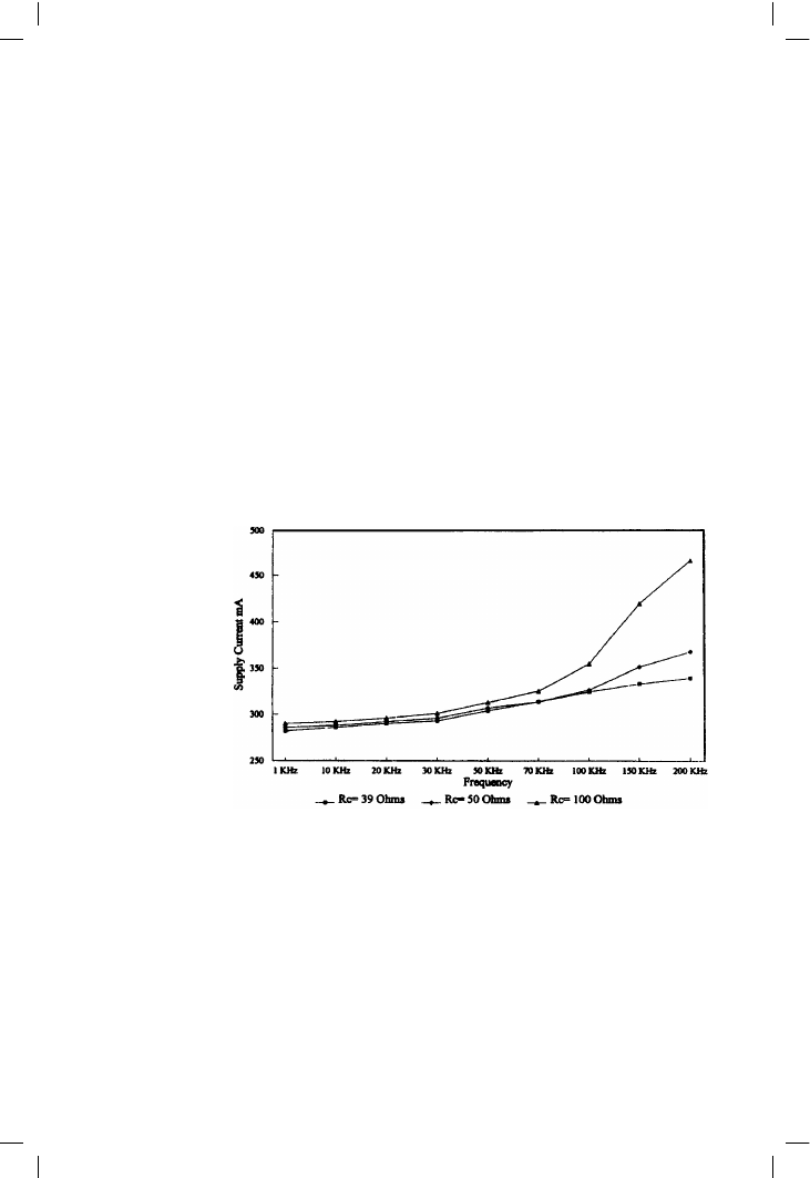
. To illustrate this, Figure 5.45 shows a graph of current
consumption vs frequency for varying driver collector resistance, for a CFP
type output.
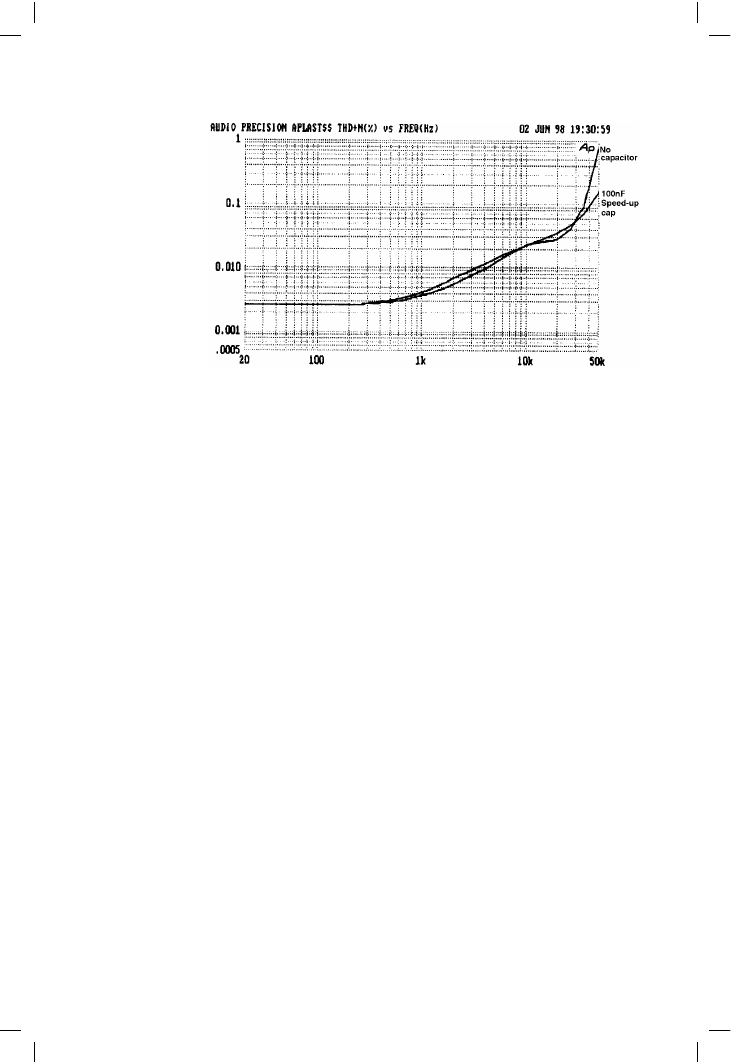
Figure 5.46 shows the reduction of HF THD by adding a speedup capacitor
across the common driver resistor of an EF Type II. At LF the difference is
small, but at 40 kHz THD is halved, indicating much cleaner switchoff.
There is also a small benefit over the range 300 Hz–8 kHz.
Thermal distortion
Thermal distortion is that caused by cyclic temperature changes at signal
frequency, causing corresponding modulation of device parameters. While
it is certainly a real problem in IC op-amps, which have input and output
153
Figure 5.45
Power supply current
versus freq, for a CFP
output with the driver
collector resistors
varied. There is little
to be gained from
reducing Rc below
50 !

Audio Power Amplifier Design Handbook
devices in very close thermal proximity, the situation in a normal discrete-
component power amplifier is quite different, and thermal distortion
cannot be detected. Having studied in detail distortion mechanisms that are
all too real, it comes as some relief to find that one prospective distortion
is illusory. Some writers appear to take it as given that such a distortion
mechanism exists in power amplifiers, but having studied the subject in
some depth I have yet to see the effect, and quite frankly I don’t think it
exists.
While now and again there have been odd mentions of thermal distortion
in power amps in some of the hi-fi press, you will never find:
1 any explanation of how it might work,
2 any estimate of the magnitude of the effect,
3 a circuit that will demonstrate its production.
In the usual absence of specific theories, one can only assume that the
alleged mechanism induces parameter changes in semiconductors whose
power dissipation varies over a cycle. If this were to happen, it would
presumably manifest itself as a rise in second or third harmonic distortion
at very low frequencies, but this simply does not happen. The largest effects
would be expected in Class-B output stages where dissipation varies wildly
over a cycle; the effect is still wholly absent.
One reason for this may be that drivers and output devices have relatively
large junctions with high thermal inertia – a few seconds with a hammer
and chisel revealed that an MJE340 driver has a chip with four times the
total area of a TL072. Given this thermal mass, parameters presumably
cannot change much even at 10 Hz. Low frequencies are also where the
global NFB factor is at its maximum; it is perfectly possible to design an
amplifier with 100 dB of feedback at 10 Hz, though much more modest
figures are sufficient to make distortion unmeasurably low up to 1 kHz or
154
Figure 5.46
HF THD reduction by
adding speedup
capacitance across
the common driver
resistance of a
Type II EF output
stage