ВУЗ: Казахская Национальная Академия Искусств им. Т. Жургенова
Категория: Учебное пособие
Дисциплина: Не указана
Добавлен: 03.02.2019
Просмотров: 17411
Скачиваний: 18

The output stage I
so. Using my design methodology a Blameless amplifier can be straightfor-
wardly designed to produce less than 0.0006% THD at 10 Hz (150 W/8 !)
without even considering thermal distortion; this suggests that we have
here a non-problem.
I accept that it is not uncommon to see amplifier THD plots that rise at low
frequencies; but whenever I have been able to investigate this, the LF rise
could be eliminated by attending to either defective decoupling or
feedback-capacitor distortion. Any thermal distortion must be at a very low
level as it is invisible at 0.0006%; remember that this is the level of a THD
reading that is visually pure noise, though there are real amplifier distortion
products buried in it.
I have therefore done some deeper investigation by spectrum analysis of
the residual, which enables the harmonics to be extracted from the noise.
The test amplifier was an optimally-biased Class-B machine very similar to
that on Figure 6.16, except with a CFP output. The Audio Precision
oscillator is very, very clean but this amplifier tests it to its limits, and so
Table 5.5 below shows harmonics in a before-and-after-amplifier compar-
ison. The spectrum analyser bandwidth was 1 Hz for 10 Hz tests, and
4.5 Hz for 1 kHz, to discriminate against wideband noise.
This further peeling of the distortion onion shows several things; that the AP is
a brilliant piece of machinery, and that the amplifier is really quite linear too.
However there is nothing resembling evidence for thermal distortion effects.
As a final argument, consider the distortion residual of a slightly
underbiased power-amp, using a CFP output configuration so that output
155
Table 5.5 Relative amplitute of distortion harmonics
10 Hz AP out · · · · Amp out
1 kHz AP out · · · · Amp out
Fundamental
.00013%
.00031%
.00012%
.00035%
Second
.00033%
.00092%
.00008%
.00060%
Third
.00035%
.00050%
.000013%
.00024%
Fourth
<.000002%
.00035%
<.000008%
.00048%
Fifth
<.00025%
<.00045%
.000014%
.00024%
Sixth
<.000006%
.00030%
.000008%
.00021%
Seventh
<.000006%
<.00008%
.000009%
.00009%
Eighth
<.000003%
.00003%
.000008%
.00016%
Ninth
<.000004%
.00011%
.000007%
<.00008%
AP THD reading
(80 kHz bandwidth)
.00046%
.00095%
.00060%
.00117%
NB: The rejection of the fundamental is not perfect, and this is shown as it contributes to the THD figure.

Audio Power Amplifier Design Handbook
device junction temperatures do not affect the quiescent current; it
therefore depends only on the driver temperatures. When the amplifier is
switched on and begins to apply sinewave power to a load, the crossover
spikes (generated by the deliberate underbiasing) will be seen to slowly
shrink in height over a couple of minutes as the drivers warm up. This
occurs even with the usual temperature compensation system, because of
the delays and losses in heating up the Vbe-multiplier transistor.
The size of these crossover spikes gives in effect a continuous readout of
driver temperature, and the slow variations that are seen imply time-
constants measured in tens of seconds or more; this must mean a negligible
response at 10 Hz.
There is no doubt that long-term thermal effects can alter Class-B amplifier
distortion, because as I have written elsewhere, the quiescent current
setting is critical for the lowest possible high-frequency THD. However this
is strictly a slow (several minutes) phenomenon, whereas enthusiasts for
thermal distortion are thinking of the usual sort of per-cycle distortion.
The above arguments lead me to conclude that thermal distortion as usually
described does not exist at a detectable level.
Thermal distortion in a power amp IC
Audio writers sometimes speculate about ‘thermal distortion’. This is
assumed to be caused by cyclic temperature changes at signal frequency,
causing modulation of transistor parameters. It is undoubtedly a real
problem in power ICs, which have input and output devices in close
thermal proximity on the same piece of sillcon, but in a discrete-
component power amplifier there is no such thermal coupling, and no such
distortion.
Thermal non-linearities would presumably appear as second or third
harmonic distortion rising at low frequencies, and the largest effects should
be in Class-B output stages where dissipation varies greatly over a cycle.
There is absolutely no such effect to be seen in discrete-component power
amplifiers.
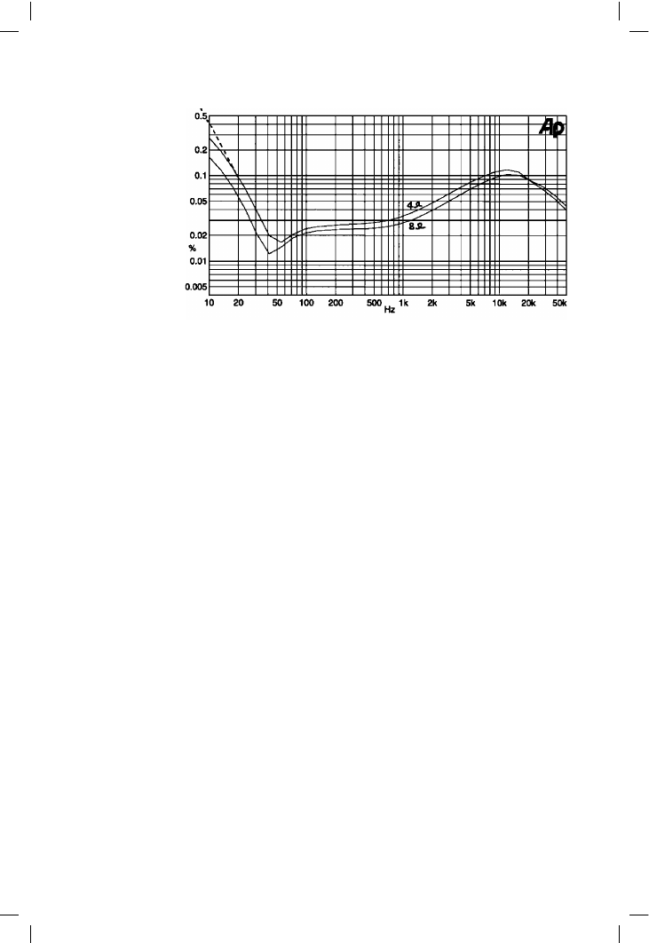
But thermal distortion certainly does exist in IC power amplifiers. Figure
5.47 is a distortion plot for the Philips TDA 1522Q power amp IC, which
I believe shows the effect. The power level was 4.4 W into 8 !, 8 W into
4 !. As is usual for such amplifiers, the distortion is generally high, but
drops into a notch at 40 Hz; the only feasible explanation for this is
cancellation of distortion products from two separate distortion sources. At
frequencies below this notch there is second-harmonic distortion rising at
12 dB/octave as frequency falls. The LF residual looks quite different from
the midband distortion, which was a mixture of second and third harmonic
plus crossover spikes.
156

The output stage I
The THD figure falls above 10 kHz because of the 80 kHz bandwidth
limitation on the residual, and the high-order nature of the harmonics that
make up crossover distortion.
All other possible sources of an LF distortion rise, such as inadequate
decoupling, were excluded. There was no output capacitor to introduce
non-linearity.
It seems pretty clear that the steep rise here is due to thermal distortion, in
the form of feedback from the power output stage to earlier parts of the
amplifier – probably the input stage. As would be expected, the effect is
greater with a heavier load which causes more heating; in fact halving the
load doubles the THD reading below the 40 Hz notch.
Selecting an output stage
Even if we stick to the most conventional of output stages, there are still an
embarrassingly large number to choose form. The cost of a complementary
pair of power FETs is currently at least twice that of roughly equivalent BJTs,
and taken with the poor linearity and low efficiency of these devices, the
use of them may require a marketing rather than a technical motivation.
Turning to BJTs, I conclude that there are the following candidates for Best
Output Stage:
1 the Emitter-Follower Type II output stage is the best at coping with
switchoff distortion but the quiescent-current stability may be
doubtful,
2 the CFP topology has good quiescent stability and low LSN; its worst
drawback is that reverse-biasing the output bases for fast switchoff is
impossible without additional HT rails,
3 the quasi-complementary-with-Baxandall-diode stage comes close to
mimicking the EF-type stages in linearity, with a potential for cost-saving
on output devices. Quiescent stability is not as good as the CFP.
157
Figure 5.47
Distortion plot for the
Phllips TDA1522Q
IC. Power out was
4.4 W rms into 8 !,
8 W rms into 4 !. The
dotted line shows a
12 dB/octave slope

Audio Power Amplifier Design Handbook
Closing the loop: distortion in complete amplifiers
In Chapter 4 it was shown how relatively simple design rules could ensure
that the THD of the small-signal stages alone could be reduced to less than
0.001% across the audio band, in a thoroughly repeatable fashion, and
without using frightening amounts of negative feedback. Combining this
sub-system with one of the more linear output stages described in Chapter
4, such as the CFP version which gives 0.014% THD open-loop, and
bearing in mind that ample NFB is available, it seems we have all the
ingredients for a virtually distortionless power amplifier. However, life is
rarely so simple . . .
(Note – the AP plots in Figures 5.5–5.7 were taken at 100 W rms into 8 !,
from an amplifier with an input error of –70 dB at 10 kHz and a c/l gain of
27 dB, giving a feedback factor of 43 dB at this frequency. This is well above
the dominant-pole frequency and so the NFB factor is dropping at 6 dB/
octave and will be down to 37 dB at 20 kHz. My experience suggests that
this is about as much feedback as is safe for general hi-fi usage, assuming
an output inductor to improve stability with capacitative loads. Sadly,
published data on this touchy topic seems to be non-existent).
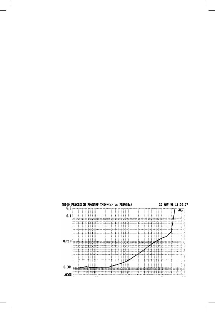
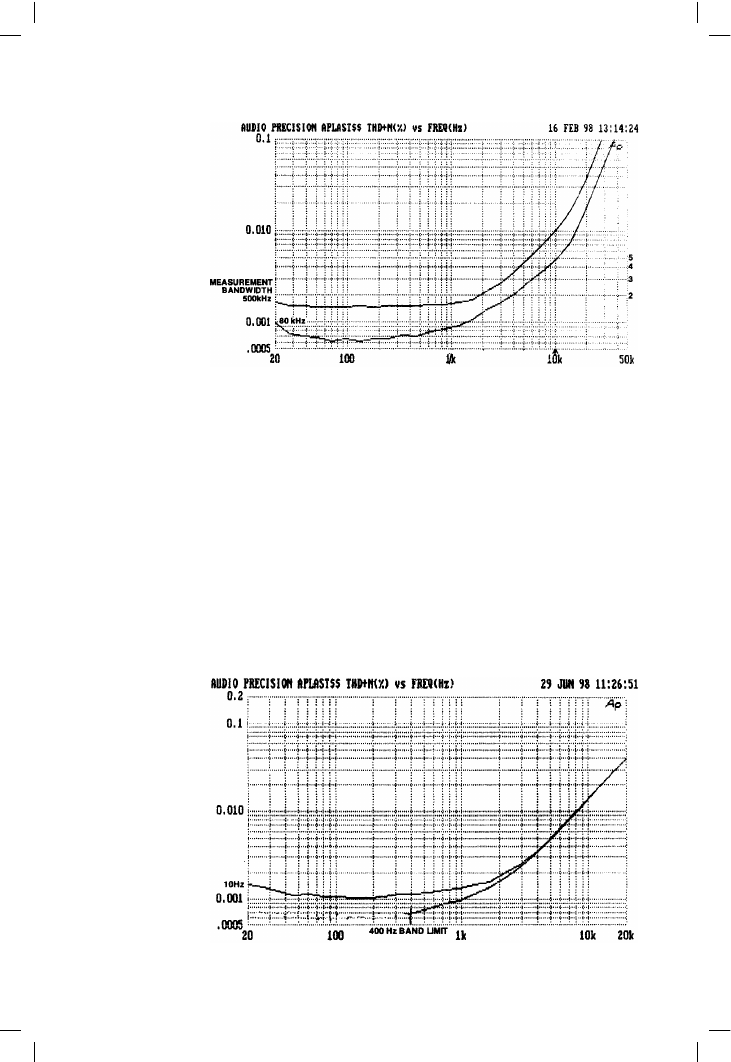
Figure 5.48 shows the distortion performance of such a closed-loop
amplifier with an EF output stage, Figure 5.49 showing the same with a CFP
output stage. Figure 5.50 shows the THD of a quasi-complementary stage
with Baxandall diode
[14]
. In each case Distortion 1, Distortion 2 and
Distortion 4–Distortion 7 have been eliminated, by methods described in
past and future chapters, to make the amplifier Blameless.
It will be seen at once that these amplifiers are not distortionless, though
the performance is markedly superior to the usual run of hardware. THD
in the LF region is very low, well below a noise floor of 0.0007%, and the
usual rise below 100 Hz is very small indeed. However, above 2 kHz,
158
Figure 5.48
Closed-loop amplifier
performance with
Emitter-Follower output
stage. 100 W into
8 !

The output stage I
THD rises with frequency at between 6 and 12 dB/octave, and the
distortion residual in this region is clearly time-aligned with the crossover
region, and consists of high-order harmonics rather than second or third.
It is intriguing to note that the quasi-Bax output gives about the same HF
THD as the EF topology, which confirms the statement on page 119 that
the addition of a Baxandall diode essentially turns a conventional quasi-
complementary stage with serious crossover asymmetry into a reasonable
emulation of a complementary EF stage. There is less HF THD with a
CFP output; this cannot be due to large-signal non-linearity as this is
negligible with an 8 ! load for all three stages, and so it must be due to
high-order crossover products.
The distortion figures given in this book are rather lower than usual. I would
like to emphasise that these are not freakish or unrepeatable figures; they
159
Figure 5.49
Closed-loop amplifier
performance with
CFP output. 100 W
into 8 !
Figure 5.50
Closed-loop amplifier
performance; quasi-
complementary
output stage with
Baxandall diode.
100 W into 8 !