ВУЗ: Казахская Национальная Академия Искусств им. Т. Жургенова
Категория: Учебное пособие
Дисциплина: Не указана
Добавлен: 03.02.2019
Просмотров: 17414
Скачиваний: 18

Power supplies and PSRR
Looking at Figure 8.2, we must assume that any connection to either HT rail
is a possible entry point for ripple injection. The PSRR behaviour for each
rail is quite different, so the two rails are examined separately.
Positive supply-rail rejection
The V+ rail injection points that must be eyed warily are the input-pair tail
and the VAS collector load. There is little temptation to use a simple resistor
tail for the input; the cost saving is negligible and the ripple performance
inadequate, even with a decoupled mid-point. A practical value for such a
tail-resistor would be 22k, which in SPICE simulation gives a low-
frequency PSRR of –120 dB for an undegenerated differential pair with
current-mirror.
Replacing this tail resistor with the usual current source improves this to
–164 dB, assuming the source has a clean bias voltage. The improvement of
44 dB is directly attributable to the greater output impedance of a current
source compared with a tail resistor; with the values shown this is 4.6 M,
and 4.6 M/22k is 46 dB, which is a very reasonable agreement. Since the
rail signal is unlikely to exceed +10 dBu, this would result in a maximum
output ripple of –154 dBu.
The measured noise floor of a real amplifier, (ripple excluded) was
–94.2 dBu (EIN = –121.4 dBu) which is mostly Johnson noise from the
emitter degeneration resistors and the global NFB network. The tail ripple
contribution would be therefore 60 dB below the noise, where I think it is
safe to neglect it.
However, the tail-source bias voltage in reality will not be perfect; it will be
developed from V+, with ripple hopefully excluded. The classic method is
a pair of silicon diodes; LED biasing provides excellent temperature
compensation, but such accuracy in setting DC conditions is probably
unnecessary. It may be desirable to bias the VAS collector current-source
from the same voltage, which rules out anything above a volt or two. A 10 V
zener might be appropriate for biasing the tail-source (given suitable
precautions against noise generation) but this would seriously curtail the
positive VAS voltage swing.
The negative-feedback biasing system used in the design in Chapter 6
provides a better basic PSRR than diodes, at the cost of some beta-
dependence. It is not quite as good as an LED, but the lower voltage
generated is more suitable for biasing a VAS source. These differences
become academic if the bias chain mid-point is filtered with 47 µF to V+,
as Table 8.1 shows; this is C11 in Figure 8.2.
As another example, the Figure 8.2 amplifier with diode-biasing and no
bias chain filtering gives an output ripple of –74 dBu; with 47 µF filtering
245

Audio Power Amplifier Design Handbook
this improves to –92 dBu, and 220 µF drops the reading into limbo below
the noise floor.
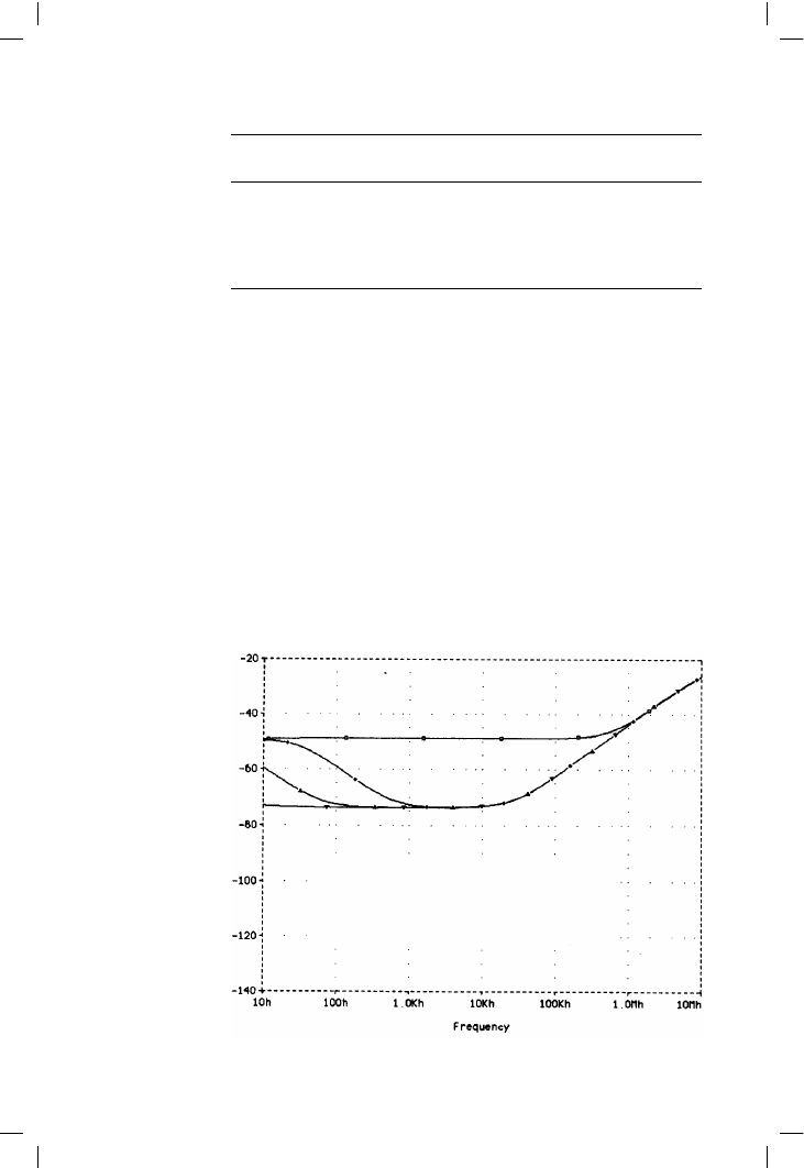
Figure 8.3 shows PSpice simulation of Figure 8.2, with a 0 dB sinewave
superimposed on V+ only. A large Cdecouple (such as 100 µF) improves LF
PSRR by about 20 dB, which should drop the residual ripple below the
noise. However, there remains another frequency-insensitive mechanism at
about –70 dB. The study of PSRR greatly resembles the peeling of onions,
because there is layer after layer, and often tears . . . There also remains an
HF injection route, starting at about 100 kHz in Figure 8.3, which is quite
unaffected by the bias-chain decoupling.
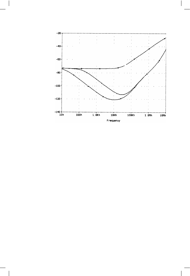
Rather than digging deeper into the precise mechanisms of the next layer,
it is simplest to RC filter the V+ supply to the input pair only (it makes very
little difference if the VAS source is decoupled or not) as a few volts lost
246
Table 8.1
No decouple
Decoupled with 47 µF
2 diodes
–65 dB
–87 dB
LED
–77 dB
–86 dB
NFB low-beta
–74 dB
–86 dB
NFB high-beta
–77 dB
–86 dB
Figure 8.3
Positive-rail rejection;
decoupling the tail
current-source bias
chain R21, R22 with
0, 1, 10 and 100 µF

Power supplies and PSRR
Negative supply-rail rejection
The V– rail is the major route for injection, and a tough nut to analyse. The
well-tried Wolf-Fence approach is to divide the problem in half, and in this
case, the Fence is erected by applying RC filtering to the small-signal
section (i.e. input current-mirror and VAS emitter) leaving the unity-gain
output stage fully exposed to rail ripple. The output ripple promptly
disappears, indicating that our wolf is getting in via the VAS or the bottom
of the input pair, or both, and the output stage is effectively immune. We
can do no more fencing of this kind, for the mirror has to be at the same DC
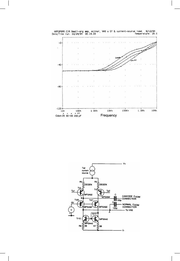
potential as the VAS. SPICE simulation of the amplifier 1 with 1 V (0 dBV)
AC signal on V– gives the PSRR curves in Figure 8.5, with Cdom stepped
in value. As before there are two regimes, one flat at –50 dB, and one rising
at 6 dB per octave, implying at least two separate injection mechanisms.
This suspicion is powerfully reinforced because as Cdom is increased, the
HF PSRR around 100 kHz improves to a maximum and then degrades
again; i.e. there is an optimum value for Cdom at about 100 pF, indicating
some sort of cancellation effect. (In the V+ case, the value of Cdom made
very little difference.)
247
here are of no consequence. Figure 8.4 shows the very beneficial effect of
this at middle frequencies, where the ear is most sensitive to ripple
components.
Figure 8.4
Positive-rail rejection;
with input-stage supply-
rail RC filtered with
100 ! and 0, 10 and
100 µF. Same scale as
Figure 8.3

Audio Power Amplifier Design Handbook
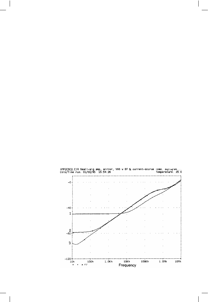
A primary LF ripple injection mechanism is Early Effect in the input-pair
transistors, which determines the –50 dB LF floor of Curve 1 in Figure 8.7,
for the standard input circuit (as per Figure 8.5 with Cdom = 100 pF).
To remove this effect, a cascode structure can be added to the input stage,
as in Figure 8.6. This holds the Vce of the input pair at a constant 5 V, and
gives Curve 2 in Figure 8.7. The LF floor is now 30 dB lower, although HF
248
Figure 8.5
Negative-rail rejection
varies with Cdom in a
complex fashion;
100 pF is the optimal
value. This implies
some sort of
concellation effect
Figure 8.6
A cascoded input
stage; Q21, Q22
prevent AC on V– from
reaching TR2, TR3
collectors, and improve
LF PSRR. B is the
alternative Cdom
connection point for
cascode compensation

Power supplies and PSRR
PSRR is slightly worse. The response to Cdom’s value is now monotonic;
simply a matter of more Cdom, less PSRR. This is a good indication that one
of two partly-cancelling injection mechanisms has been deactivated.
There is a deep subtlety hidden here. It is natural to assume that Early effect
in the input pair is changing the signal current fed from the input stage to
the VAS, but it is not so; this current is in fact completely unaltered. What
is changed is the integrity of the feedback subtraction performed by the
input pair; modulating the Vce of TR1, TR2 causes the output to alter at LF
by global feedback action. Varying the amount of Early effect in TR1, TR2
by modifying VAF (Early intercept voltage) in the PSpice transistor model
alters the floor height for Curve 1; the worst injection is with the lowest VAF
(i.e. Vce has maximum effect on lc) which makes sense.
We still have a LF floor, though it is now at –80 rather than –50 dB.
Extensive experimentation showed that this is getting in via the collector
supply of TR12, the VAS beta-enhancer, modulating Vce and adding a
signal to the inner VAS loop by early effect once more. This is easily
squished by decoupling TR12 collector to V–, and the LF floor drops to
about –95 dB, where I think we can leave it for the time being. (Curve 3 in
Figure 8.7.)
Having peeled two layers from the LF PSRR onion, something needs to be
done about the rising injection with frequency above 100 Hz. Looking
again at Figure 8.2, the VAS immediately attracts attention as an entry
249
Figure 8.7
Curve 1 is negative-rail
PSRR for the standard
input. Curve 2 shows
how cascoding the
input stage improves
rail rejection. Curve 3
shows further
improvement by also
decoupling TR12
collector to V–