ВУЗ: Казахская Национальная Академия Искусств им. Т. Жургенова
Категория: Учебное пособие
Дисциплина: Не указана
Добавлен: 03.02.2019
Просмотров: 17413
Скачиваний: 18
Audio Power Amplifier Design Handbook
route. It is often glibly stated that such stages suffer from ripple fed in
directly through Cdom, which certainly looks a prime suspect, connected
as it is from V– to the VAS collector. However, this bald statement is untrue.
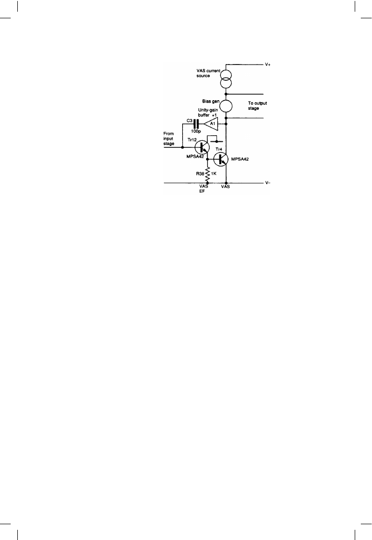
In simulation it is possible to insert an ideal unity-gain buffer between the
VAS collector and Cdom, without stability problems (A1 in Figure 8.8) and
this absolutely prevents direct signal flow from V– to VAS collector through
Cdom; the PSRR is completely unchanged.
Cdom has been eliminated as a direct conduit for ripple injection, but the
PSRR remains very sensitive to its value. In fact the NFB factor available is
the determining factor in suppressing V– ripple-injection, and the two
quantities are often numerically equal across the audio band.
The conventional amplifier architecture we are examining inevitably has
the VAS sitting on one supply-rail; full voltage swing would otherwise be
impossible. Therefore the VAS input must be referenced to V–, and it is very
likely that this change-of-reference from ground to V– is the basic source of
injection. At first sight, it is hard to work out just what the VAS collector
signal is referenced to, since this circuit node consists of two transistor
collectors facing each other, with nothing to determine where it sits; the
answer is that the global NFB references it to ground.
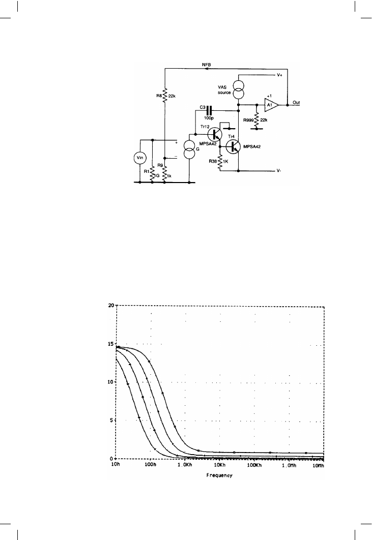
Consider an amplifier reduced to the conceptual model in Figure 8.9, with
a real VAS combined with a perfect transconductance stage G, and unity-
gain buffer A1. The VAS beta-enhancer TR12 must be included, as it proves
to have a powerful effect on LF PSRR.
To start with, the global NFB is temporarily removed, and a DC input
voltage is critically set to keep the amplifier in the active region (an easy
trick in simulation). As frequency increases, the local NFB through Cdom
becomes steadily more effective, and the impedance at the VAS collector
250
Figure 8.8
Adding a Cdom buffer
A1 to prevent any
possibility of signal
entering directly from
the V– rail
Power supplies and PSRR
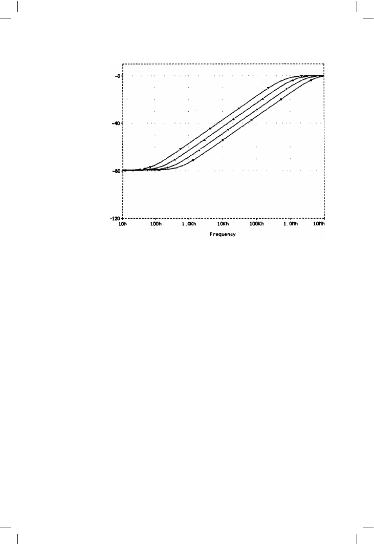
falls. Therefore the VAS collector becomes more and more closely bound
to the AC on V–, until at a sufficiently high frequency (typically 10 kHz) the
PSRR converges on 0 dB, and everything on the V– rail couples straight
through at unity gain, as shown in Figure 8.10.
There is an extra complication here; the TR12/TR4 combination actually
shows gain from V– to the output at low frequencies; this is due to Early
effect, mostly in TR12. If TR12 was omitted the LF open-loop gain drops to
about –6 dB.
251
Figure 8.9
A conceptual SPICE
model for V– PSRR,
with only the VAS
made from real
components. R999
represents VAS loading
Figure 8.10
Open-loop PSRR from
the model in Figure
8.8, with Cdom
value stepped. There
is actual gain below
1 kHz
Audio Power Amplifier Design Handbook
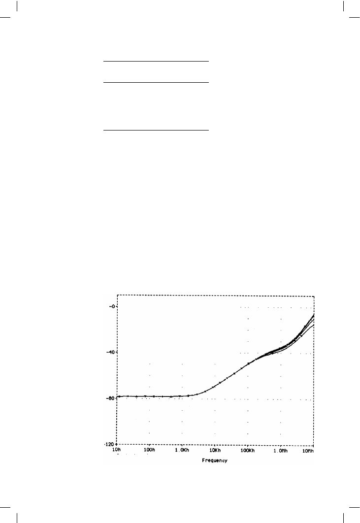
Reconnecting the global NFB, Figure 8.11 shows a good emulation of the
PSRR for the complete amplifier in Figure 8.7. The 10–15 dB open-loop-
gain is flattened out by the global NFB, and no trace of it can be seen in
Figure 8.11.
Now the NFB attempts to determine the amplifier output via the VAS
collector, and if this control was perfect the PSRR would be infinite. It is not,
because the NFB factor is finite, and falls with rising frequency, so PSRR
deteriorates at exactly the same rate as the open-loop gain falls. This can be
seen on many op-amp spec sheets, where V– PSRR falls off from the
dominant-pole frequency, assuming conventional op-amp design with a
VAS on V–.
Clearly a high global NFB factor at LF is vital to keep out V– disturbances.
In Chapter 4 I rather tendentiously suggested that apparent open-loop
bandwidth could be extended quite remarkably (without changing the
amount of NFB at HF where it matters) by reducing LF loop gain; a high-
value resistor Rnfb in parallel with Cdom works the trick. What I did not say
was that a high global NFB factor at LF is also invaluable for keeping the
hum out; a point overlooked by those advocating low NFB factors as a
matter of faith rather than reason.
Table 8.2 shows how reducing global NFB by decreasing the value of Rnfb
degraded ripple rejection in a real amplifier.
252
Figure 8.11
Closed-loop PSRR from
Figure 8.9, with Cdom
stepped to alter the
closed-loop NFB factor
Power supplies and PSRR
Having got to the bottom of the V– PSRR mechanism, in a just world our
reward would be a new and elegant way of preventing such ripple
injection. Such a method indeed exists, though I believe it has never before
been applied to power amplifiers
[5],[6]
. The trick is to change the reference,
as far as Cdom is concerned, to ground. Figure 8.6 shows that cascode-
compensation can be implemented simply by connecting Cdom to point B
rather than the usual VAS base connection at A. Figure 8.12 demonstrates
that this is effective, PSRR at 1 kHz improving by about 20 dB.
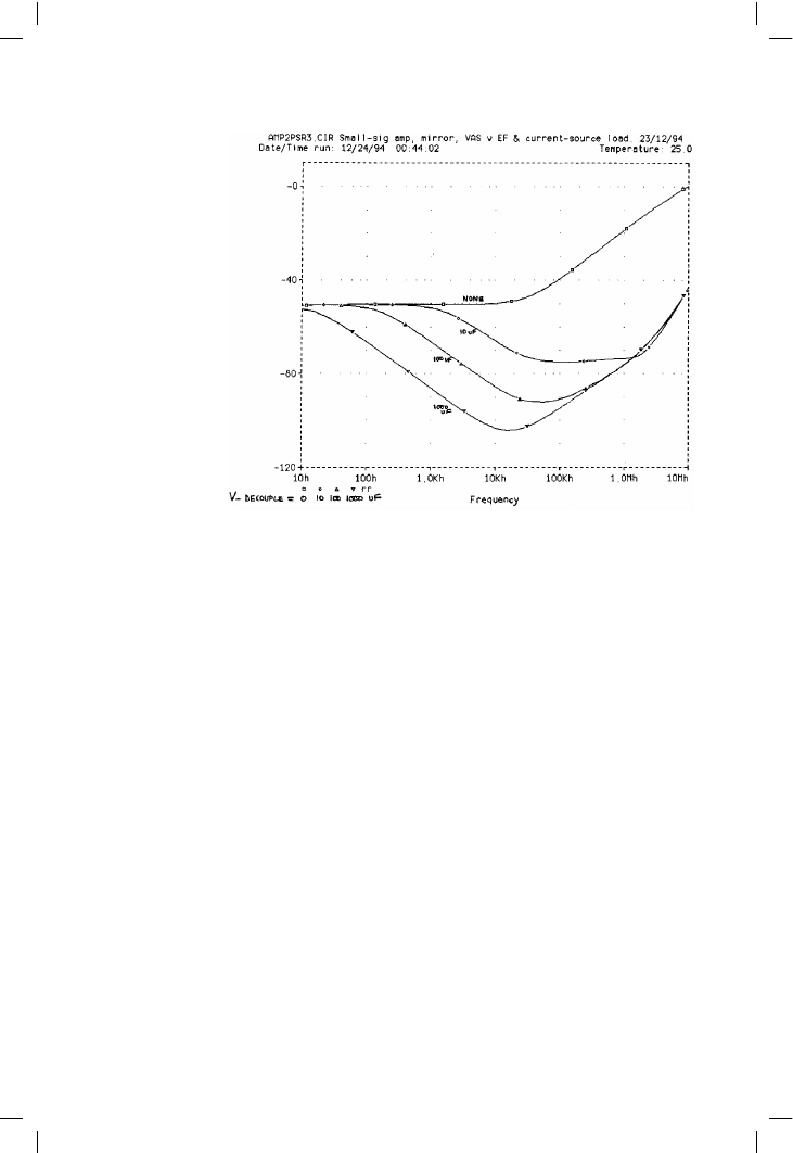
Elegant or not, the simplest way to reduce ripple below the noise floor still
seems to be brute-force RC filtering of the V– supply to the input mirror and
VAS, removing the disturbances before they enter. It may be crude, but it is
effective, as shown in Figure 8.13. Good LF PSRR requires a large RC time-
constant, and the response at DC is naturally unimproved, but the real snag
is that the necessary voltage drop across R directly reduces amplifier output
253
Table 8.2
Rnfb
Ripple Out
None
83.3 dBu
470k
85.0 dBu
200k
80.1 dBu
100k
73.9 dBu
Figure 8.12
Using an input
cascode to change the
reference for Cdom.
The LF PSRR is
unchanged, but
extends much higher in
frequency. (Compare
Curve 2 in Figure
8.7.) Note that Cdom
value now has little
effect
Audio Power Amplifier Design Handbook
swing, and since the magic number of watts available depends on voltage
squared, it can make a surprising difference to the raw commercial
numbers (though not, of course, to perceived loudness). With the circuit
values shown 10 ! is about the maximum tolerable value; even this gives
a measurable reduction in output. The accompanying C should be at least
220 µF, and a higher value is desirable if every trace of ripple is to be
removed.
References
1. Sinclair (ed) Audio and Hi-Fi Handbook pub Newnes 1993, p. 541.
2. Linsley-Hood, J Evolutionary Audio. Part 3 Electronics World, Jan 1990,
p. 18.
3. Williams, T EMC For Product Designers pub Newnes (Butterworth-
Heinemann) 1992, ISBN 0 7506 1264 9 p. 106.
4. Ball, G Distorting Power Supplies EW+WW, Dec 90, p. 1084.
5. Ribner and Copeland Design Techniques for Cascoded CMOS Opamps
IEEE J. Solid-State Circuits, Dec 1984, p. 919.
6. Ahuja, B K Improved Frequency Compensation Technique for CMOS
Opamps. IEEE J. Solid-State Circuits, Dec 1983, pp. 629–633.
254
Figure 8.13
RC filtering of the V–
rail is effective at
medium frequencies,
but less good at LF,
even with 100 µF of
filtering. R = 10 !