ВУЗ: Казахская Национальная Академия Искусств им. Т. Жургенова
Категория: Учебное пособие
Дисциплина: Не указана
Добавлен: 03.02.2019
Просмотров: 17409
Скачиваний: 18

Audio Power Amplifier Design Handbook
The constancy of this sum-of-currents is important because it shows that the
voltage measured across Re1 and Re2 together is also effectively constant
so long as the amplifier stays in Class-A. This in turn means that quiescent
current can be simply set with a constant-voltage bias generator, in very
much the same way as Class-B.
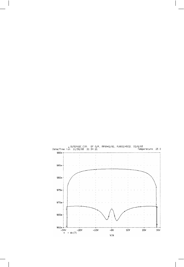
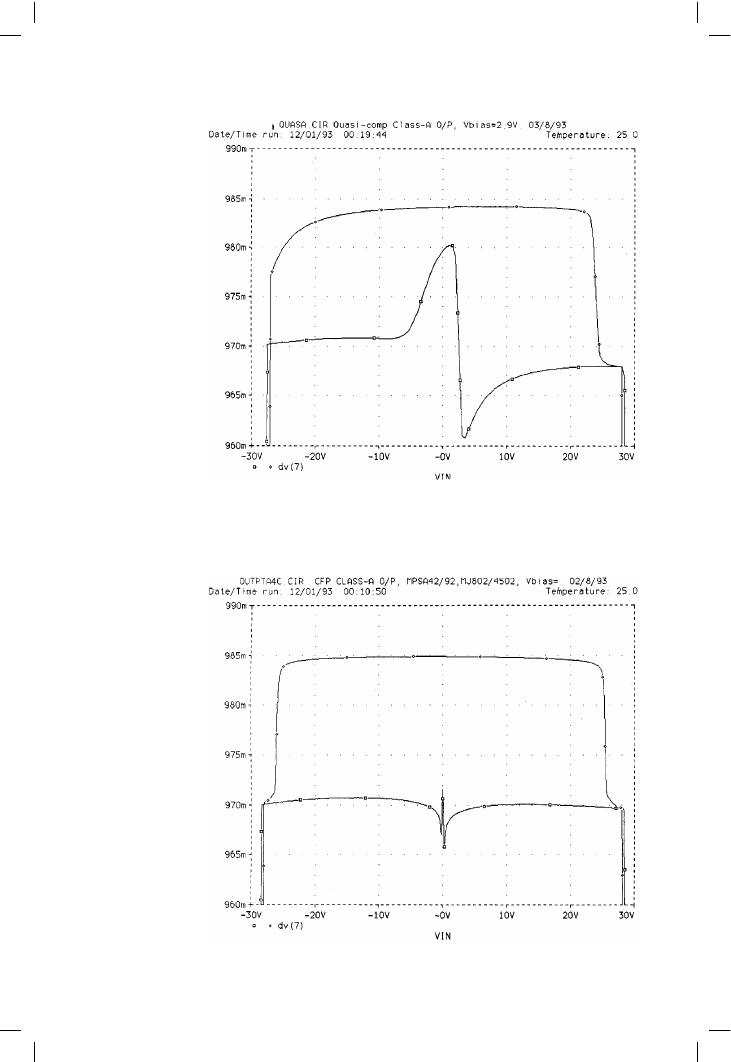
Figures 9.3, 9.4 and 9.5 show Spice gain plots for open-loop output stages,
with 8 ! loading and 1.6 A quiescent; the circuitry is exactly as for Class-B
in Chapter 6. The upper traces show Class-A gain, and the lower traces
optimal-bias Class-B gain for comparison. Figure 9.3 shows an emitter-
follower output, Figure 9.4 a simple quasi-complementary stage, and
Figure 9.5 a CFP output.
We would expect Class-A stages to be more linear than B, and they are.
(Harmonic and THD figures for the three configurations, at 20 V Pk, are
shown in Table 9.1.) There is absolutely no gain wobble around 0 V, as in
Class-B, and push-pull Class-A really can and does cancel even-order
distortion.
It is at once clear that the emitter-follower has more gain variation, and
therefore worse linearity, than the CFP, while the quasi-comp circuit shows
an interesting mix of the two. The more curved side of the quasi gain plot
is on the –ve side, where the CFP half of the quasi circuit is passing most of
the current; however we know by comparing Figure 9.3 and Figure 9.5 that
the CFP is the more linear structure. Therefore it appears that the shape of
260
Figure 9.3
Gain linearity of the
Class-A emitter-follower
output stage. Load is
8 !, and quiescent
current (Iq) is 1.6 A

Class-A power amplifiers
Figure 9.4
Gain linearity of the
Class-A quasi-
complementary output
stage. Conditions as
Figure 9.3
Figure 9.5
Gain linearity of the
Class-A CFP output
stage
261

Audio Power Amplifier Design Handbook
the gain curve is determined by the output half that is turning off,
presumably because this shows the biggest gm changes. The CFP structure
maintains gm better as current decreases, and so gives a flatter gain curve
with less rounding of the extremes.
The gain behaviour of these stages is reflected in their harmonic generation;
Table 9.1 reveals that the two symmetrical topologies give mostly odd-
order harmonics, as expected. The asymmetry of the quasi-comp version
causes a large increase in even-order harmonics, and this is reflected in the
higher THD figure. Nonetheless all the THD figures are still 2 to 3 times
lower than for their Class-B equivalents.
This modest factor of improvement may seem a poor return for the extra
dissipation of Class-A, but not so. The crucial point about the distortion
from a Class-A output stage is not just that it is low in magnitude, but that
it is low-order, and so benefits much more from the typical NFB factor that
falls with frequency than does high-order crossover distortion.
The choice of Class-A output topology is now simple. For best perform-
ance, use the CFP; apart from greater basic linearity, the effects of output
device temperature on Iq are servoed-out by local feedback, as in Class B.
For utmost economy, use the quasi-complementary with two NPN devices;
these need only a low Vce(max) for a typical Class-A amp, so here is an
opportunity to recoup some of the money spent on heatsinking. The rules
here are somewhat different from Class-B; the simple quasi-complementary
configuration gives first-class results with moderate NFB, and adding a
Baxandall diode to simulate a complementary emitter-follower stage gives
little improvement in linearity. See however Nelson-Jones
[7]
for an example
of its use.
It is sometimes assumed that the different mode of operation of Class-A
makes it inherently short-circuit proof. This may be true with some
configurations, but the high-biased type studied here will continue
delivering current in time-honoured Class-B fashion until it bursts, and
overload protection seems to be no less essential.
262
Table 9.1
Harmonic:
Emitter Follower
Quasi-Comp
CFP Output
Second
.00012%
.0118%
.00095%
Third
.0095%
.0064%
.0025%
Fourth
.00006%
.0011%
.00012%
Fifth
.00080%
.00058%
.00029%
THD
.0095%
.0135%
.0027%
(THD is calculated from the first nine harmonics, though levels above the fifth are
very small)

Class-A power amplifiers
Quiescent current control systems
Unlike Class-B, precise control of quiescent current is not required to
optimise distortion; for good linearity there just has to be enough of it.
However, the Iq must be under some control to prevent thermal runaway,
particularly if the emitter-follower output is used. A badly designed
quiescent controller can ruin the linearity, and careful design is required.
There is also the point that a precisely held standing-current is considered
the mark of a well-bred Class-A amplifier; a quiescent that lurches around
like a drunken sailor does not inspire confidence.
Straightforward thermal compensation with a Vbe-multiplier bias generator
works
[8]
, and will prevent thermal runaway. However, unlike Class-B,
Class-A gives the opportunity of tightly controlling Iq by negative feedback.
This is profoundly ironic because now that we can precisely control Iq, it
is no longer critical. Nevertheless it seems churlish to ignore the
opportunity, and so feedback quiescent control will be examined.
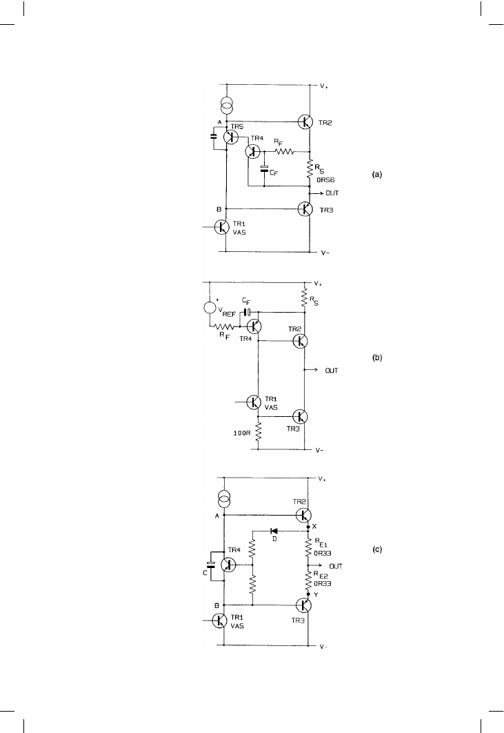
There are two basic methods of feedback current-control. In the first, the
current in one output device is monitored, either by measuring the voltage
across one emitter-resistor (Rs in Figure 9.6a), or by a collector sensing
resistor; the second method monitors the sum of the device currents, which
as described above, is constant in Class-A.
The first method as implemented in Figure 9.6a
[7]
compares the Vbe of TR4
with the voltage across R
s
, with filtering by RF, CF. If quiescent is excessive,
then TR4 conducts more, turning on TR5 and reducing the bias voltage
between points A and B. In Figure 9.6b, which uses the VCIS approach, the
voltage across collector sensing resistor Rs is compared with Vref by TR4,
the value of Vref being chosen to allow for TR4 Vbe
[9]
. Filtering is once
more by RF, CF.
For either Figure 9.6a or b, the current being monitored contains large
amounts of signal, and must be low-pass filtered before being used for control
purposes. This is awkward as it adds one more time-constant to worry about if
the amplifier is driven into asymmetrical clipping. In the case of collector-
sensing there are unavoidable losses in the extra sense resistor. It is also my
experience that imperfect filtering causes a serious rise in LF distortion.
The Better Way is to monitor current in both emitter resistors; as explained
above, the voltage across both is very nearly constant, and in practice
filtering is unnecessary. An example of this approach is shown in Figure 9.6c,
based on a concept originated by Nelson Pass
[10]
. Here TR4 compares its
own Vbe with the voltage between X and B; excessive quiescent turns on
TR4 and reduces the bias directly. Diode D is not essential to the concept, but
usefully increases the current-feedback loop-gain; omitting it more than
doubles Iq variation with TR7 temperature in the Pass circuit.
The trouble with this method is that TR3 Vbe directly affects the bias setting,
but is outside the current-control loop. A multiple of Vbe is established
263

Audio Power Amplifier Design Handbook
Figure 9.6
Current-control systems.
Only that at c avoids
the need to low-pass
filter the control signal;
C simply provides
feedforward to speed
up signal transfer to
TR2
264