ВУЗ: Казахская Национальная Академия Искусств им. Т. Жургенова
Категория: Учебное пособие
Дисциплина: Не указана
Добавлен: 03.02.2019
Просмотров: 17406
Скачиваний: 18

Class-A power amplifiers
between X and B, when what we really want to control is the voltage
between X and Y. The temperature variations of TR4 and TR3 Vbe partly
cancel, but only partly. This method is best used with a CFP or quasi output so
that the difference between Y and B depends only on the driver temperature,
which can be kept low. The reference is TR4 Vbe, which is itself temperature-
dependent; even if it is kept away from the hot bits it will react to ambient
temperature changes, and this explains the poor performance of the Pass
method for global temp changes (Table 9.2).
A novel quiescent current controller
To solve this problem, I would like to introduce the novel control method
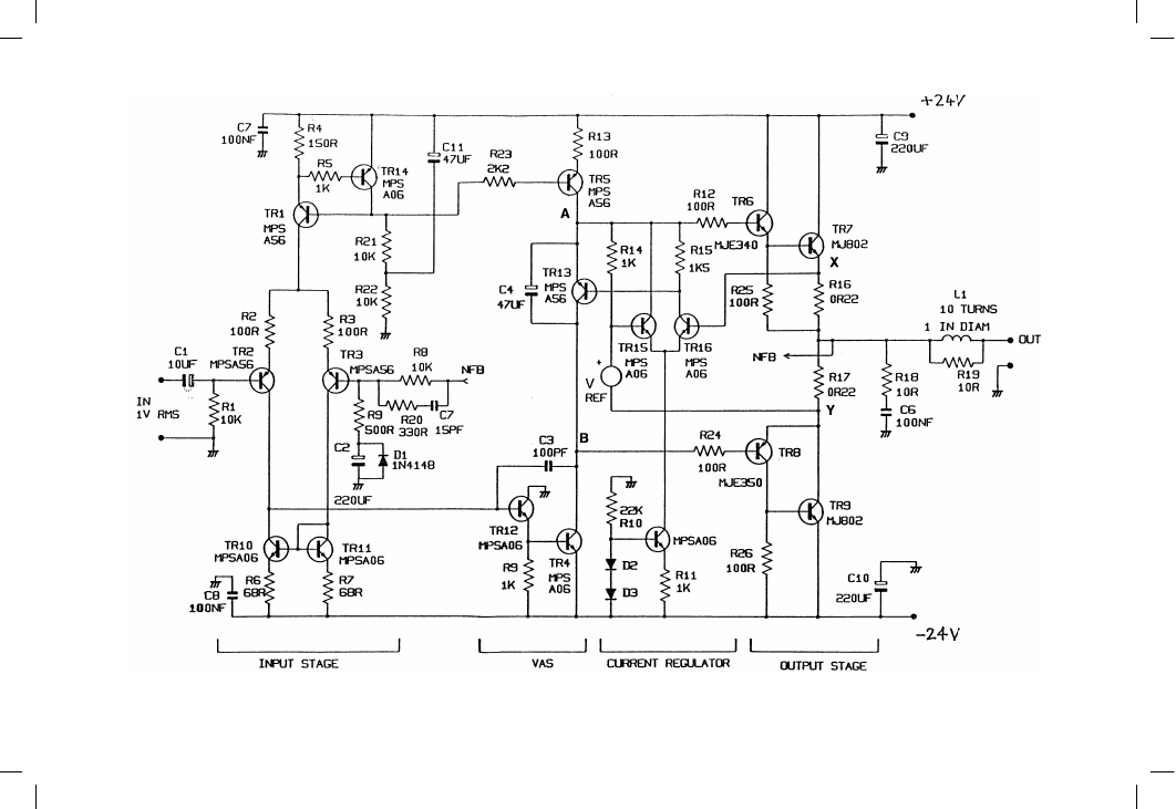
in Figure 9.7. We need to compare the floating voltage between X and Y
with a fixed reference, which sounds like a requirement for two differential
amplifiers. This can be reduced to one by sitting the reference Vref on point
Y; this is a very low-impedance point and can easily swallow a reference
current of 1 mA or so. A simple differential pair TR15, 16 then compares the
reference voltage with that at point Y; excess quiescent turns on TR16,
causing TR13 to conduct more and reducing the bias voltage.
The circuitry looks enigmatic because of the high-impedance of TR13
collector would seem to prevent signal from reaching the upper half of the
output stage; this is in essence true, but the vital point is that TR13 is part
of an NFB loop that establishes a voltage at A that will keep the bias voltage
between A and B constant. This comes to the same thing as maintaining a
constant Vbias across TR5. As might be imagined, this loop does not shine
at transferring signals quickly, and this duty is done by feed-forward
capacitor C4. Without it, the loop (rather surprisingly) works correctly, but
HF oscillation at some part of the cycle is almost certain. With C4 in place
the current-loop does not need to move quickly, since it is not required to
transfer signal but rather to maintain a DC level.
The experimental study of Iq stability is not easy because of the inaccess-
ibility of junction temperatures. Professional SPICE implementations like
265
Table 9.2
Iq change per
degree C
Changing
TR7 temp only
Changing
Global temp
Quasi + Vbe-mult
+0.112%
–0.43%
Pass: as Figure 9.6c
+0.0257%
–14.1%
Pass: no diode D
+0.0675%
–10.7%
New system:
+0.006%
–0.038%
(assuming OR22 emitter resistors and 1.6 A Iq)

Figure 9.7
A Blameless 20 W Class-A power amplifier, using the novel current-control system
266

Class-A power amplifiers
PSpice allow both the global circuit temperature and the temperature of
individual devices to be manipulated; this is another aspect where sim-
ulators shine. The exact relationships of component temperatures in an
amplifier is hard to predict, so I show here only the results of changing the
global temperature of all devices, and changing the junction temp of TR7
alone (Figure 9.7) with different current-controllers. TR7 will be one of the
hottest transistors and unlike TR9 it is not in a local NFB loop, which would
greatly reduce its thermal effects.
A Class-A design
A design example of a Blameless 20 W/8 ! Class-A power amplifier is
shown in Figure 9.7. This is as close as possible in operating parameters to
the previous Class-B design, to aid comparison; in particular the NFB factor
remains 30 dB at 20 kHz. The front-end is as for the Class-B version, which
should not be surprising as it does exactly the same job, input Distortion 1
being unaffected by output topology. As before the input pair uses a high
tail current, so that R2, 3 can be introduced to linearise the transfer
characteristic and set the transconductance. Distortion 2 (VAS) is dealt with
as before, the beta-enhancer TR12 increasing the local feedback through
Cdom. There is no need to worry about Distortion 4 (non-linear loading by
output stage) as the input impedance of a Class-A output, while not
constant, does not have the sharp variations shown by Class-B.
Figure 9.7 uses a standard quasi output. This may be replaced by a CFP
stage without problems. In both cases the distortion is extremely low, but
gratifyingly the CFP proves even better than the quasi, confirming the
simulation results for output stages in isolation.
The operation of the current regulator TR13, 15, 16 has already been
described. The reference used is a National LM385/1.2. Its output voltage
is fixed at 1.223 V nominal; this is reduced to approx. 0.6 V by a 1k–1k
divider (not shown). Using this band-gap reference, a 1.6 A Iq is held to
within +/–2 mA from a second or two after switch-on. Looking at Table 9.2,
there seems no doubt that the new system is effective.
As before, a simple unregulated power supply with 10,000 µF reservoirs
was used, and despite the higher prevailing ripple, no PSRR difficulties
were encountered once the usual decoupling precautions were taken.
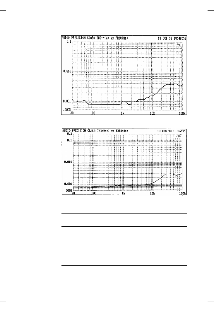
The closed-loop distortion performance (with conventional compensation)
is shown in Figure 9.8 for the quasi-comp output stage, and in Figure 9.9
for a CFP output version. The THD residual is pure noise for almost all of
the audio spectrum, and only above 10 kHz do small amounts of third-
harmonic appear. The expected source is the input pair, but this so far
remains unconfirmed.
The distortion generated by the Class-B and A design examples is
summarised in Table 9.3, which shows a pleasing reduction as various
267

Audio Power Amplifier Design Handbook
268
Figure 9.8
Class-A amplifier
THD performance
with quasi-comp
output stage. The
steps in the LF portion
of the trace are
measurement
artefacts
Figure 9.9
Class-A distortion
performance with
CFP output stage
Table 9.3
1 kHz
10 kHz
20 kHz
Power
Class B EF
<.0006%
.0060%
.012%
50 W
Class B CFP
<.0006%
.0022%
.0040%
50 W
Class B EF 2-pole
<.0006%
.0015%
.0026%
50 W
Class A quasi
<.0006%
.0017%
.0030%
20 W
Class A CFP
<.0006%
.0010%
.0018%
20 W
Class A CFP 2-pole
<.0006%
.0010%
.0012%
20 W
(All for 8 ! loads and 80 kHz bandwidth. Single-pole compensation unless otherwise
stated)

Class-A power amplifiers
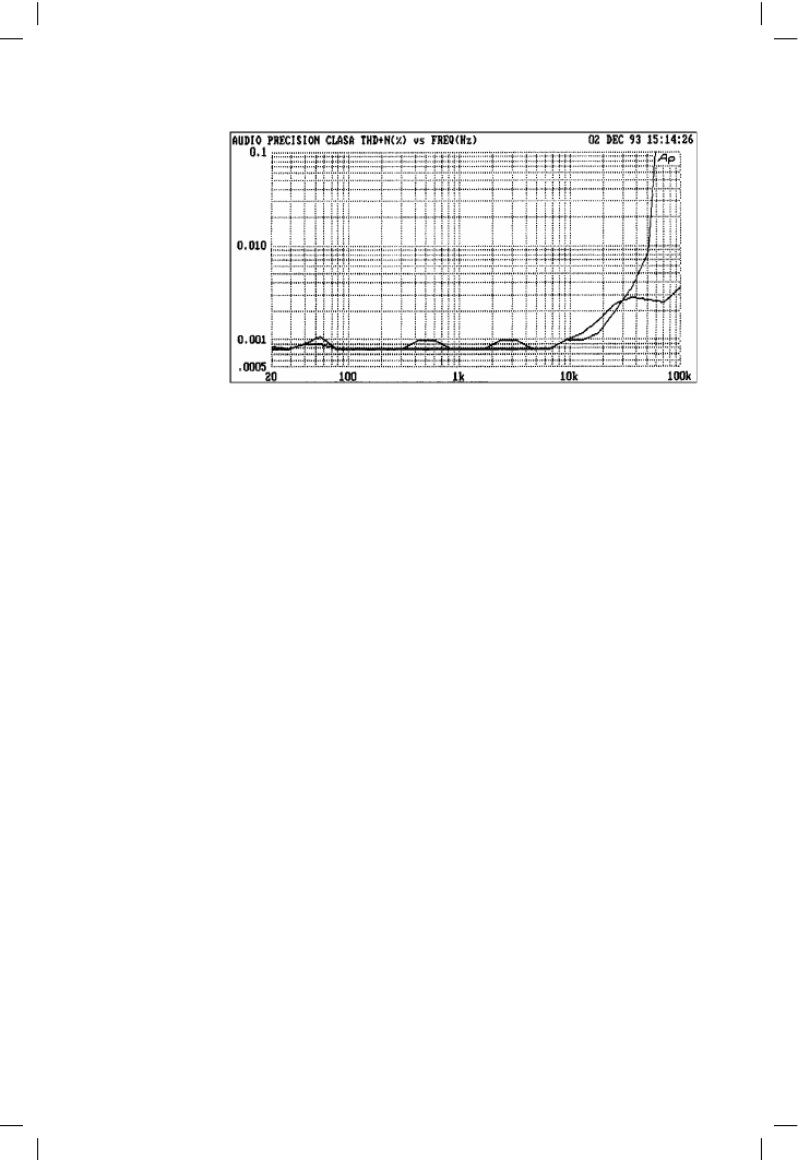
measures are taken to deal with it. As a final fling two-pole compensation
was applied to the most linear (CFP) of the Class-A versions, reducing
distortion to a rather small .0012% at 20 kHz, at some cost in slew-rate.
(Figure 9.10). While this may not be the fabled Distortionless Amplifier, it
must be a near relation . . .
The trimodal amplifier
I present here my own contribution to global warming in the shape of an
improved Class-A amplifier; it is believed to be unique in that it not only
copes with load impedance dips by means of the most linear form of Class-
AB possible, but will also operate as a Blameless Class-B engine. The
power output in pure Class-A is 20 to 30 W into 8 !, depending on the
supply-rails chosen.
This amplifier uses a Complementary-Feedback-Pair (CFP) output stage for
best possible linearity, and some incremental improvements have been
made to noise, slew-rate and maximum DC offset. The circuit naturally
bears a very close resemblance to a Blameless Class-B amplifier, and so it
was decided to retain the Class-B Vbe-multiplier, and use it as a safety-
circuit to prevent catastrophe if the relatively complex Class-A current-
regulator failed. From this the idea arose of making the amplifier instantly
switchable between Class-A and Class-B modes, which gives two kinds of
amplifier for the price of one, and permits of some interesting listening tests.
Now you really can do an A/B comparison . . .
In the Class-B mode the amplifier has the usual negligible quiescent
dissipation. In Class-A the thermal dissipation is naturally considerable, as
true Class-A operation is extended down to 6 ! resistive loads for the full
output voltage swing, by suitable choice of the quiescent current; with
heavier loading the amplifier gracefully enters Class-AB, in which it will
give full output down to 3 ! before the Safe-Operating-Area (SOAR)
269
Figure 9.10
Distortion
performance for CFP
output stage with
2-pole compensation.
The THD drops to
0.0012% at 20 kHz,
but the extra VAS
loading has
compromised the
positive-going slew
capability