ВУЗ: Казахская Национальная Академия Искусств им. Т. Жургенова
Категория: Учебное пособие
Дисциплина: Не указана
Добавлен: 03.02.2019
Просмотров: 17404
Скачиваний: 18

Audio Power Amplifier Design Handbook
limiting begins to act. Output into 2 ! is severely curtailed, as it must be
with one output pair, and this kind of load is definitely not
recommended.
In short, the amplifier allows a choice between:
1 being very linear all the time (Blameless Class-B) and
2 ultra-linear most of the time (Class-A) with occasional excursions into
Class-AB. The AB mode is still extremely linear by current standards,
though inherently it can never be quite as good as properly-handled
Class-B. Since there are three classes of operation I have decided to call
the design a trimodal power amplifier.
It is impossible to be sure that you have read all the literature; however, to
the best of my knowledge this is the first ever Trimodal amplifier.
As previously said, designing a low-distortion Class-A amplifier is in
general a good deal simpler than the same exercise for Class-B, as all the
difficulties of arranging the best possible crossover between the output
devices disappear. Because of this it is hard to define exactly what
Blameless means for a Class-A amplifier. In Class-B the situation is quite
different, and Blameless has a very specific meaning; when each of the
eight or more distortion mechanisms has been minimised in effect, there
always remains the crossover distortion inherent in Class-B, and there
appears to be no way to reduce it without departing radically from what
might be called the generic Lin amplifier configuration. Therefore the
Blameless state appears to represent some sort of theoretical limit for Class-
B, but not for Class-A.
However, Class-B considerations cannot be ignored, even in a design
intended to be Class-A only, because if the amplifier does find itself driving
a lower load impedance than expected, it will move into Class-AB, and
then all the additional Class-B requirements are just as significant as for a
Class-B design proper. Class-AB can never give distortion as low as
optimally-biased Class-B, but it can be made to approach it reasonably
closely, if the extra distortion mechanisms are correctly handled.
In a class-A amplifier, certain sacrifices are made in the name of quality,
and so it is reasonable not to be satisfied with anything less than the best
possible linearity. The amplifier described here therefore uses the Com-
plementary-Feedback-Pair (CFP) type of output stage, which has the
lowest distortion due to the local feedback loops wrapped around the
output devices. It also has the advantage of better output efficiency than
the emitter-follower (EF) version, and inherently superior quiescent
current stability. It will shortly be seen that these are both important for
this design.
Half-serious thought was given to labelling the Class-A mode Distortionless
as the THD is completely unmeasurable across most of the audio band.
270

Class-A power amplifiers
However, detectable distortion products do exist above 10 kHz, so this
provocative idea was regretfully abandoned.
It seemed appropriate to take another look at the Class-A design, to see if
it could be inched a few steps nearer perfection. The result is a slight
improvement in efficiency, and a 2 dB improvement in noise performance.
In addition the expected range of output DC offset has been reduced from
+/–50 mV to +/–15 mV, still without any adjustment.
Load impedance and operating mode
The amplifier is 4 ! capable in both A/AB and B operating modes, though
it is the nature of things that the distortion performance is not quite so good.
All solid-state amplifiers (without qualification, as far as I am aware) are
much happier with an 8 ! load, both in terms of linearity and efficiency;
loudspeaker designers please note. With a 4 ! load, Class-B operation
gives better THD than Class-A/AB, because the latter will always be in AB
mode, and therefore generating extra output stage distortion through gm-
doubling. (Which should really be called gain-deficit-halving, but some-
how I don’t see this term catching on.) These not entirely obvious
relationships are summarised in Table 9.4.
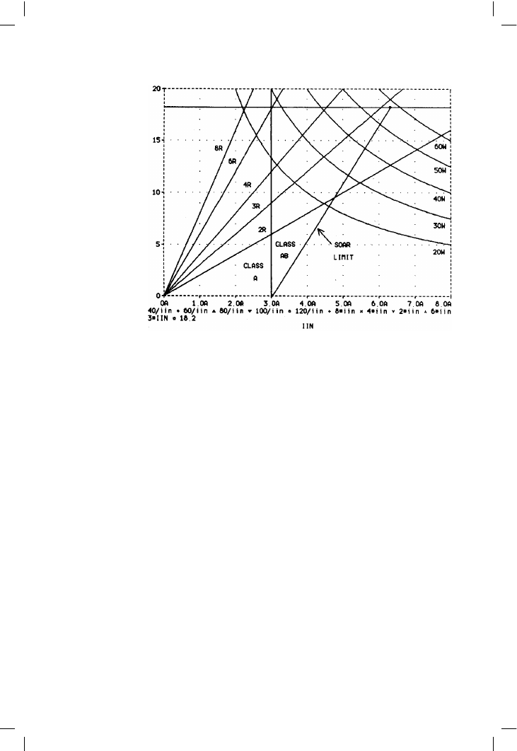
Figure 9.11 attempts to show diagrammatically just how power, load
resistance, and operating mode are related. The rails have been set to
+/–20 V, which just allows 20 W into 8 ! in Class-A. The curves are lines
of constant power (i.e. V
× I in the load), the upper horizontal line
represents maximum voltage output, allowing for Vce(sat)s, and the sloping
line on the right is the SOAR protection locus; the output can never move
outside this area in either mode. The intersection between the load
resistance lines sloping up from the origin and the ultimate limits of
voltage-clip and SOAR protection define which of the curved constant-
power lines is reached.
271
Table 9.4
Load
Mode
Distortion
Dissipation
8 !
A/AB
Very low
High
4 !
A/AB
High
High
8 !
B
Low
Low
4 !
B
Medium
Medium
(Note: High distortion in the context of this sort of amplifier means about 0.002%
THD at 1 kHz and 0.01% at 10 kHz)

Audio Power Amplifier Design Handbook
In A/AB mode, the operating point must be left of the vertical push-pull
current-limit line (at 3 A, twice the quiescent current) for Class-A. If we
move to the right of this limit along one of the impedance lines, the output
devices will begin turning off for part of the cycle; this is the AB operation
zone. In Class-B mode, the 3 A line has no significance and the amplifier
remains in optimal Class-B until clipping or SOAR limiting occurs. Note
that the diagram axes represent instantaneous power in the load, but the
curves show sinewave RMS power, and that is the reason for the apparent
factor-of-two discrepancy between them.
272
Figure 9.11
The relationships
between load,
mode, and power
output. The
intersection between
the sloping load
resistance lines and
the ultimate limits of
voltage-clipping and
SOAR protection
define which of the
curved constant-
power lines is
reached. In A/AB
mode, the operating
point must be to the
left of the vertical
push-pull current-limit
line for true Class-A
Efficiency
Concern for efficiency in Class-A may seem paradoxical, but one way of
looking at it is that Class-A Watts are precious things, wrought in great heat
and dissipation, and so for a given quiescent power it makes sense to
ensure that the amplifier approaches its limited theoretical efficiency as
closely as possible. I was confirmed in this course by reading of another
recent design
[11]
which seems to throw efficiency to the winds by using a
hybrid BJT/FET cascode output stage. The voltage losses inherent in this
arrangement demand +/–50 V rails and six-fold output devices for a 100 W
Class-A capability; such rail voltages would give 156 W from a 100%
efficient amplifier.
The voltage efficiency of a power amplifier is the fraction of the supply-rail
voltage which can actually be delivered as peak-to-peak voltage swing into

Class-A power amplifiers
a specified load; efficiency is invariably less into 4 ! due to the greater
resistive voltage drops with increased current.
The Class-B amplifier I described in Chapter 6 has a voltage efficiency of
91.7% for positive swings, and 92.5% for negative, into 8 !. Amplifiers are
not in general completely symmetrical, and so two figures need to be
quoted; alternatively the lower of the two can be given as this defines the
maximum undistorted sinewave. These figures above are for an emitter-
follower output stage, and a CFP output does better, the positive and
negative efficiencies being 94.0% and 94.7% respectively. The EF version
gives a lower output swing because it has two more Vbe drops in series to
be accommodated between the supply-rails; the CFP is always more
voltage-efficient, and so selecting it over the EF for the current Class-A
design is the first step in maximising efficiency.
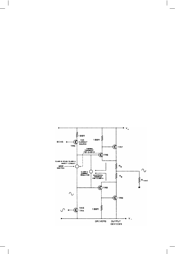
Figure 9.12 shows the basic CFP output stage, together with its two biasing
elements. In Class-A the quiescent current is rigidly controlled by negative-
feedback; this is possible because in Class-A the total voltage across both
emitter resistors Re is constant throughout the cycle. In Class-B this is not
the case, and we must rely on thermal feedback from the output stage,
though to be strictly accurate this is not feedback at all, but a kind of
feedforward (Chapter 12). Another big advantage of the CFP configuration
273
Figure 9.12
The basic CFP output
stage, equally suited to
operating Class B, AB
and A, depending on
the magnitude of
Vbias. The emitter
resistors Re may be
from 0.1 to 0.47 !

Audio Power Amplifier Design Handbook
is that Iq depends only on driver temperature, and this is important in the
Class-B mode, where true feedback control of quiescent current is not
possible, especially if low-value Re’s such as 0.1 !, are chosen, rather than
the more usual 0.22 !; the motivation for doing this will soon become
clear.
The voltage efficiency for the quasi-complementary Class-A circuit of the
circuit on page 266 into 8 ! is 89.8% positive and 92.2% negative.
Converting this to the CFP output stage increases this to 92.9% positive and
93.6% negative. Note that a Class-A quiescent current (Iq) of 1.5 A is
assumed throughout; this allows 31 W into 8 ! in push-pull, if the supply-
rails are adequately high. However the assumption that loudspeaker
impedance never drops below 8 ! is distinctly doubtful, to put it mildly,
and so as before this design allows for full Class-A output voltage swing into
loads down to 6 !.
So how else can we improve efficiency? The addition of extra and higher
supply-rails for the small-signal section of the amplifier surprisingly does
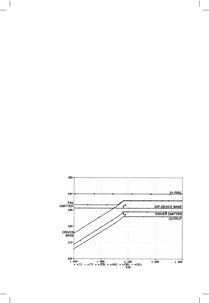
not give a significant increase in output; examination of Figure 9.13 shows
why. In this region, the output device TR6 base is at a virtually constant
880 mV from the V+ rail, and as TR7 driver base rises it passes this level,
and keeps going up; clipping has not yet occurred. The driver emitter
follows the driver base up, until the voltage difference between this emitter
and the output base (i.e. the driver Vce) becomes too small to allow further
conduction; this choke point is indicated by the arrows A–A. At this point
the driver base is forced to level off, although it is still about 500 mV below
the level of V+. Note also how the voltage between V+ and TR5 emitter
274
Figure 9.13
PSpice simulation
showing how
positive clipping
occurs in the CFP
output. A higher sub-
rail for the VAS
cannot increase the
output swing, as the
limit is set by the
minimum driver Vce,
and not the VAS
output swing