ВУЗ: Казахская Национальная Академия Искусств им. Т. Жургенова
Категория: Учебное пособие
Дисциплина: Не указана
Добавлен: 03.02.2019
Просмотров: 17402
Скачиваний: 18

Class-A power amplifiers
collapses. Thus a higher rail will give no extra voltage swing, which I must
admit came as something of a surprise. Higher sub-rails for small-signal
sections only come into their own in FET amplifiers, where the high Vgs for
FET conduction (5 V or more) makes their use almost mandatory.
The efficiency figures given so far are all greater for negative rather than
positive voltage swings. The approach to the rail for negative clipping is
slightly closer because there is no equivalent to the 0.6 V bias established
across R13; however this advantage is absorbed by the need to lose a little
voltage in the RC filtering of the V– supply to the current-mirror and VAS.
This is essential if really good ripple/hum performance is to be obtained
(see Chapter 8).
In the quest for efficiency, an obvious variable is the value of the output
emitter resistors Re. The performance of the current-regulator described,
especially when combined with a CFP output stage, is more than good
enough to allow these resistors to be reduced while retaining first-class Iq
stability. I took 0.1 ! as the lowest practicable value, and even this is
comparable with PCB track resistance, so some care in the exact details of
physical layout is essential; in particular the emitter resistors must be
treated as four-terminal components to exclude unwanted voltage drops in
the tracks leading to the resistor pads.
If Re is reduced from 0.22 ! to 0.1 ! then voltage efficiency improves from
92.9%/93.6%, to 94.2%/95.0%. Is this improvement worth having? Well,
the voltage-limited power output into 8 ! is increased from 31.2 to 32.2 W
with +/–24 V rails, at zero cost, but it would be idle to pretend that the
resulting increase in SPL is highly significant; it does however provide the
philosophical satisfaction that as much Class-A power as possible is being
produced for a given dissipation; a delicate pleasure.
The linearity of the CFP output stage in Class-A is very slightly worse with
0.1 ! emitter resistors, though the difference is small and only detectable
open-loop; the simulated THD for 20 V pk–pk into 8 ! is only increased
from 0.0027% to 0.0029%. This is probably due simply to the slightly
lower total resistance seen by the output stage.
However, at the same time, reducing the emitter resistors to 0R1 provides
much lower distortion when the amplifier runs out of Class-A; it halves the
size of the step gain changes inherent in Class-AB, and so effectively
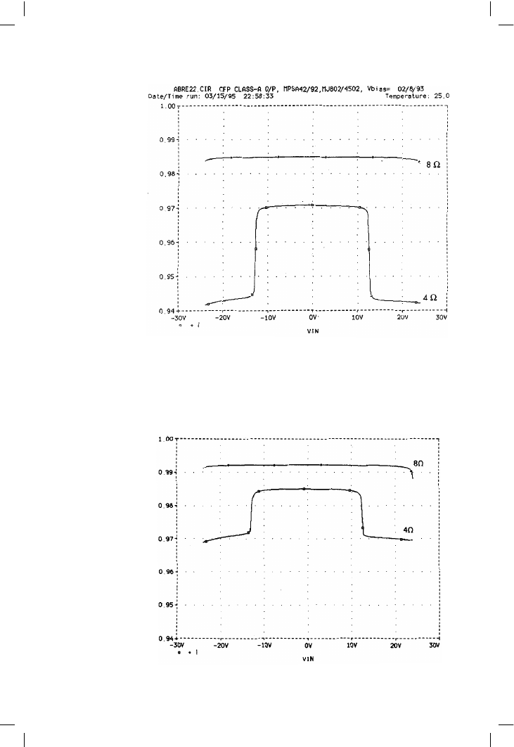
reduces distortion into 4 ! loads. See Figures 9.14 and 9.15 for output
linearity simulations; the measured results from a real and Blameless
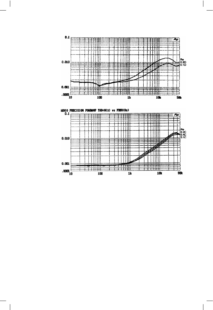
Trimodal amplifier are shown in Figure 9.16, where it can be clearly seen
that THD has been halved by this simple change. To the best of my
knowledge this is a new result; if you must work in Class-AB, then keep the
emitter resistors as low as possible, to minimise the gain changes.
Having considered the linearity of Class-A and AB, we must not neglect
what effect this radical Re change has on Class-B linearity. The answer is,
275

Audio Power Amplifier Design Handbook
Figure 9.14
CFP output stage
linearity with
Re = 0R22. Upper
trace is Class-A into
8 !, lower is Class-
AB operation into
4 !, showing step
changes in gain of
.024 units
Figure 9.15
CFP output linearity
with Re = 0R1,
re-biased to keep Iq at
1.5 A. There is slightly
poorer linearity in the
flat-topped Class-A
region than for
Re = 0R22, but the
4 ! AB steps are
halved in size at .012
units. Note that both
gains are now closer to
unity; same scale as
Figure 9.14
276

Class-A power amplifiers
not very much; see Figure 9.17, where crossover distortion seems to be
slightly higher with Re = 0.2 ! than for either 0.1 or 0.4 !. Whether this is
a consistent effect (for CFP stages anyway) remains to be seen.
The detailed mechanisms of bias control and mode-switching are
described on pages 277–282.
On Trimodal biasing
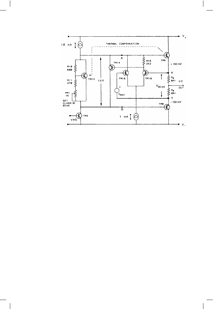
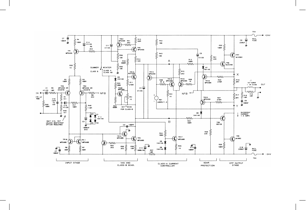
Figure 9.18 shows a simplified rendering of the Trimodal biasing system;
the full version appears in Figure 9.19. The voltage between points A and
B is determined by one of two controller systems, only one of which can be
in command at a time. Since both are basically shunt voltage regulators
sitting between A and B, the result is that the lowest voltage wins. The novel
Class-A current-controller introduced on page 265 is used here adapted for
0.1 ! emitter resistors, mainly by reducing the reference voltage to 300 mV,
which gives a quiescent current (Iq) of 1.5 A when established across the
total emitter resistance of 0.2 !.
277
Figure 9.16
Distortion in Class-AB
is reduced by
lowering the value of
Re
Figure 9.17
Proving that emitter
resistors matter much
less in Class-B. Output
was 20 W in 8 !,
with optimal bias.
Interestingly, the bias
does not need
adjusting as the value
of Re changes

Audio Power Amplifier Design Handbook
In parallel with the current-controller is the Vbe-multiplier TR13. In Class-B
mode, the current-controller is disabled, and critical biasing for minimal
crossover distortion is provided in the usual way by adjusting preset PR1 to
set the voltage across TR13. In Class-A/AB mode, the voltage TR13 attempts
to establish is increased (by shorting out PR1) to a value greater than that
required for Class-A. The current-controller therefore takes charge of the
voltage between X and Y, and unless it fails TR13 does not conduct. Points
A, B, X, and Y are the same circuit nodes as in the simple Class-A design
(see Figure 9.6c).
Class-A/AB mode
In Class-A/AB mode, the current-controller (TR14, 15, 16 in Figure 9.18) is
active and TR13 is off, as TR20 has shorted out PR1. TR15, 16 form a
simple differential amplifier that compares the reference voltage across R31
with the Vbias voltage across output emitter resistors R16 and R17; as
explained above, in Class-A this voltage remains constant despite delivery
of current into the load. If the voltage across R16, 17 tends to rise, then
TR16 conducts more, turning TR14 more on and reducing the voltage
between A and B. TR14, 15 and 16 all move up and down with the
amplifier output, and so a tail current-source (TR17) is used.
I am very aware that the current-controller is more complex than the simple
Vbe-multiplier used in most Class-B designs. There is an obvious risk that
an assembly error could cause a massive current that would prompt the
278
Figure 9.18
The simplified current-
controller in action,
showing typical DC
voltages in Class-A.
Points A, B, X and Y
are in Figure 9.6 on
page 000

Figure 9.19
The complete circuit diagram of Trimodal amplifier, including the optional bootstrapping components, R47 and C15