ВУЗ: Казахская Национальная Академия Искусств им. Т. Жургенова
Категория: Учебное пособие
Дисциплина: Не указана
Добавлен: 03.02.2019
Просмотров: 17386
Скачиваний: 18

FET output stages
– in other words drain current falls with increasing temperature – but on the
other hand the coefficient reverses sign at low drain currents, and this
implies that precise quiescent-current setting will be very difficult. A
negative-temperature coefficient provides good protection against thermal
runaway, but this should never be a problem anyway.
FET vs BJT output stages
On beginning any power amplifier design, one of the first decisions that
must be made is whether to use BJTs or FETs in the output stage. This
decision may of course already have been taken for you by the marketing
department, as the general mood of the marketplace is that if FETs are more
expensive, they must be better. If however, you are lucky enough to have
this crucial decision left to you, then FETs normally disqualify themselves
on the same grounds of price. If the extra cost is not translated into either
better performance and/or a higher sustainable price for the product, then
it appears to be foolish to choose anything other than BJTs.
Power MOSFETS are often hailed as the solution to all amplifier problems,
but they have their own drawbacks, not the least being low trans-
conductance, poor linearity, and a high ON-resistance that makes output
efficiency mediocre. The high-frequency response may be better, implying
that the second pole P2 of the amplifier response will be higher, allowing
the dominant pole P1 be raised with the same stability margin, and so in
turn giving more NFB to reduce distortion. However, we would need this
extra feedback (if it proves available in practice) to correct the worse open-
loop distortion, and even then the overall linearity would almost certainly
be worse. To complicate matters, the compensation cannot necessarily be
lighter because the higher output-resistance makes more likely the
lowering of the output pole by capacitative loading.
The extended FET frequency response is, like so many electronic swords,
two-edged if not worse, and the HF capabilities mean that rigorous care
must be taken to prevent parasitic oscillation, as this is often promptly
followed by an explosion of disconcerting violence. FETs should at least
give freedom from switchoff troubles (Distortion 3c) as they do not suffer
from BJT charge-storage effects.
Advantages of FETs
1 For a simple complementary FET output stage, drivers are not required.
This is somewhat negated by the need for gate-protection zener
diodes.
2 There is no second-breakdown failure mechanism. This may simplify the
design of overload protection systems, especially when arranging for
them to cope with highly reactive loads.
3 There are no charge-storage effects to cause switchoff distortion.
315

Audio Power Amplifier Design Handbook
Disadvantages of FETs
1 Linearity is very poor by comparison with a BJT degenerated to give the
same transconductance. The Class-B conduction characteristics do not
cross over smoothly, and there is no equivalent to the optimal Class-B
bias condition that is very obvious with a BJT output stage.
2 The Vgs required for conduction is usually of the order of 4–6 V, which
is much greater than the 0.6–0.8 V required by a BJT for base drive. This
greatly reduces the voltage efficiency of the output stage unless the
preceding small-signal stages are run from separate and higher-voltage
supply rails.
3 The minimum channel resistance of the FET, known as Rds(on), is high
and gives a further reduction in efficiency compared with BJT outputs.
4 Power FETs are liable to parasitic oscillation. In severe cases a plastic-
package device will literally explode. This is normally controllable in the
simple complementary FET output stage by adding gate-stopper resistors,
but is a serious disincentive to trying radical experiments in output stage
circuit design.
5 Some commentators claim that FET parameters are predictable; I find this
hard to understand as they are notorious for being anything but. From
one manufacturer’s data (Harris), the Vgs for the IRF240 FET varies
between 2.0 and 4.0 V for an ld of 250 µA; this is a range of two to one.
In contrast the Vbe/lc relation in bipolars is fixed by a mathematical
equation for a given transistor type, and is much more reliable. Nobody
uses FETs in log converters.
6 Since the Vgs spreads are high, this will complicate putting devices in
parallel for greater power capability. Paralleled BJT stages rarely require
current-sharing resistors of greater than 0.1 !, but for the FET case they
may need to be a good deal larger, reducing efficiency further.
7 At the time of writing, there is a significant economic penalty in
using FETs. Taking an amplifier of given power output, the cost of the
output semiconductors is increased by between 1.5 and 2 times with
FETs.
IGBTs
Insulated-Gate Bipolar Transistors represent a relatively new option for the
amplifier designer. They have been held up as combining the best features
of FETs and BJTs. In my view this is a dubious proposition as I find the
advantages of FETs for audio to be heavily outweighed by the drawbacks,
and if IGBTs have any special advantages they have not so far emerged.
According to the Toshiba application notes
[1]
, IGBTs consist of an FET
controlling a bipolar power transistor; I have no information on the linearity
of these devices, but the combination does not sound promising.
The most discouraging aspect of IGBTs is the presence of a parasitic BJT
that turns the device hard on above a critical current threshold. This inbuilt
316

Figure 11.1
Three MOSFET output
architectures
317

Audio Power Amplifier Design Handbook
self-destruct mechanism will at the very least make overload protection an
extremely critical matter; it seems unlikely that IGBTs will prove popular for
audio amplification.
Power FET output stages
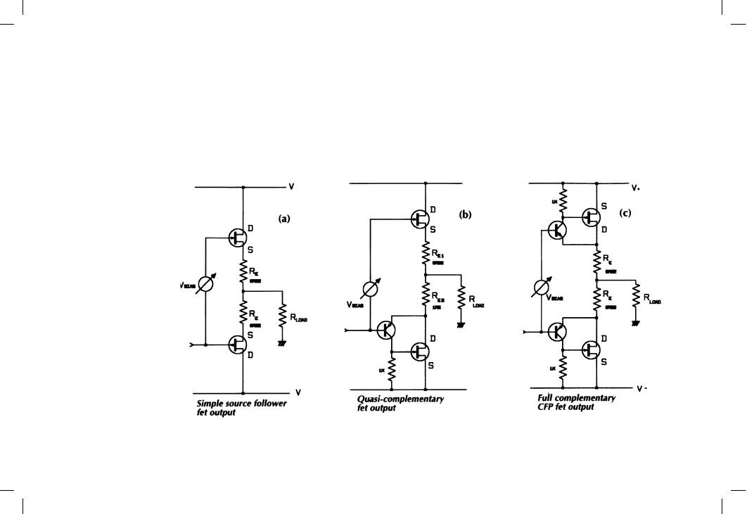
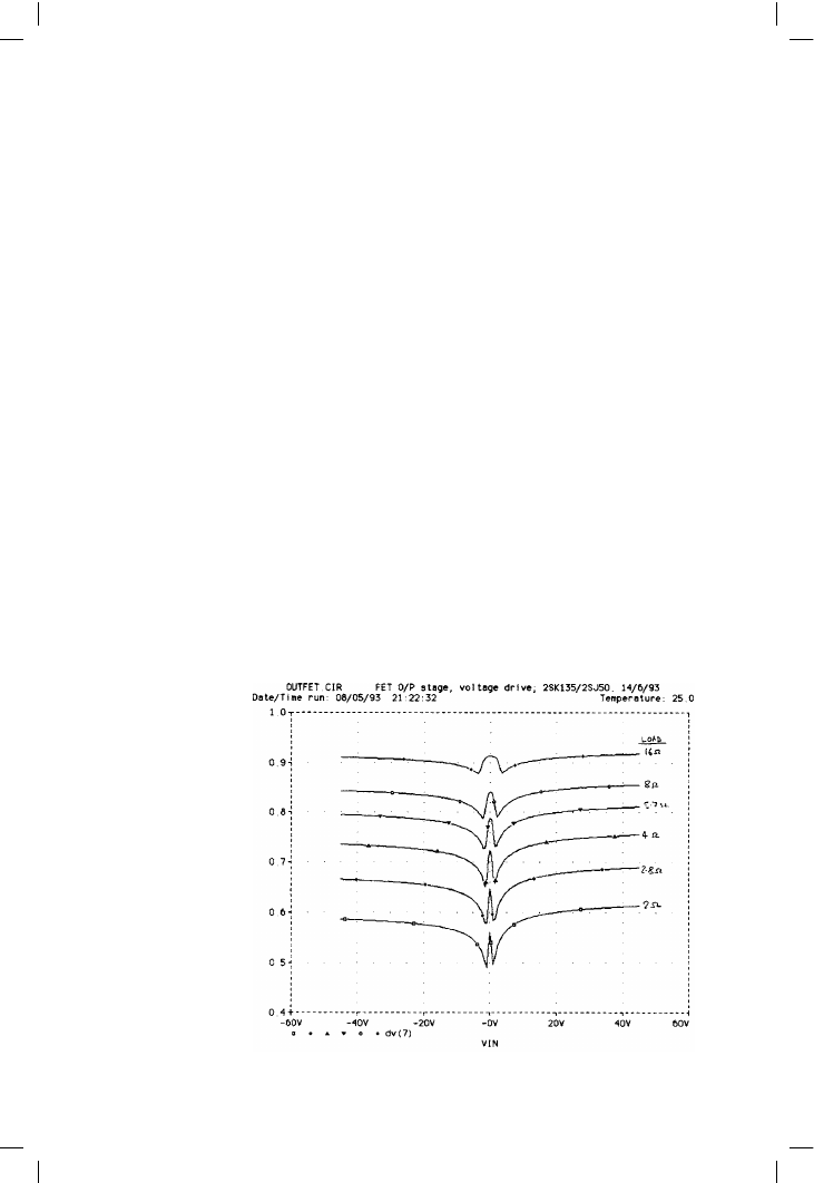
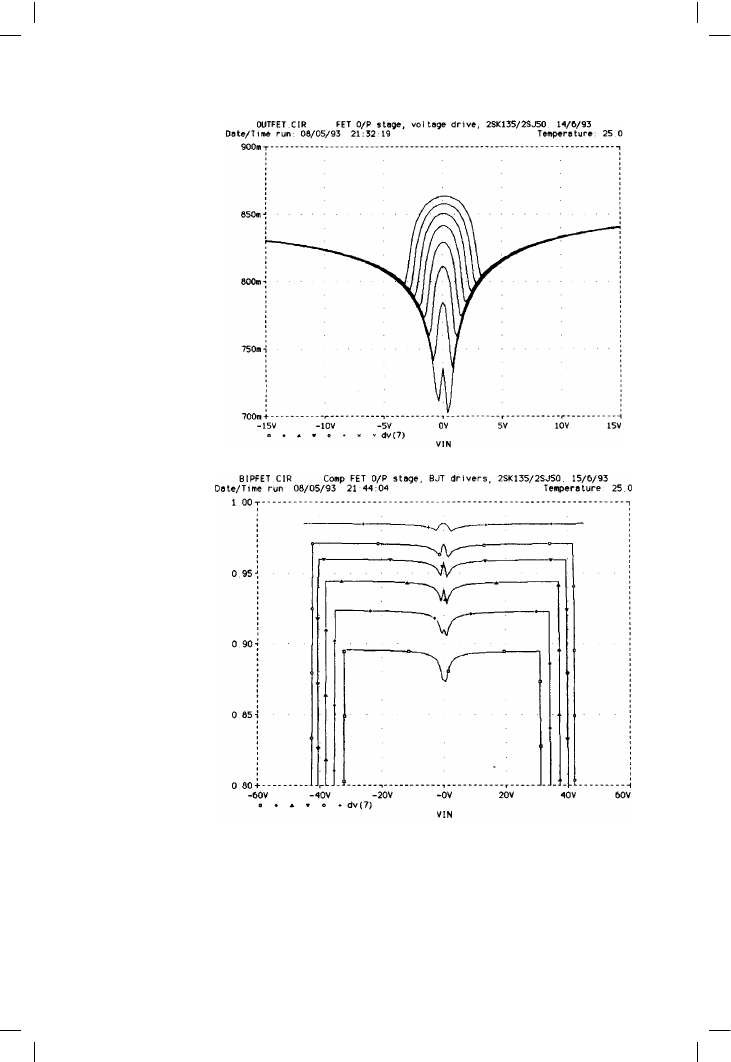
Three types of FET output stage are shown in Figure 11.1, and Figures
11.2–11.5 show SPICE gain plots, using 2SK135/2SJ50 devices. Most FET
amplifiers use the simple source-follower configuration in Figure 11.1a; the
large-signal gain plot at Figure 11.2 shows that the gain for a given load is
lower (0.83 rather than 0.97 for bipolar, at 8 !) because of low gm, and
this, with the high on-resistance, reduces output efficiency seriously. Open-
loop distortion is markedly higher; however LSN does not increase with
heavier loading, there being no equivalent of Bipolar Gain-Droop. The
crossover region has sharper and larger gain deviations than a bipolar stage,
and generally looks pretty nasty; Figure 11.3 shows the impossibility of
finding a correct Vbias setting.
Figure 11.1b shows a hybrid (i.e. bipolar/FET) quasi-complementary
output stage, first described in Self
[2]
. This topology is intended to
maximise economy rather than performance, once the decision has been
made (presumably for marketing reasons) to use FETs, by making both
output devices cheap N-channel devices; complementary MOSFET pairs
remain relatively rare and expensive. The basic configuration is badly
asymmetrical, the hybrid lower half having a higher and more constant
318
Figure 11.2
Source-Follower FET
large-signal gain vs
output

FET output stages
gain than the source-follower upper half. Increasing the value of Re2 gives
a reasonable match between the gains of the two halves, but leaves a
daunting crossover discontinuity.
The hybrid full-complementary stage in Figure 11.1c was conceived
[3]
to
maximise FET performance by linearising the output devices with local
319
Figure 11.3
Source-Follower FET
crossover region
+/–15 V range
Figure 11.4
Complementary
Bipolar-FET gain vs
output