ВУЗ: Казахская Национальная Академия Искусств им. Т. Жургенова
Категория: Учебное пособие
Дисциплина: Не указана
Добавлен: 03.02.2019
Просмотров: 17383
Скачиваний: 18

Audio Power Amplifier Design Handbook
feedback and reducing Iq variations due to the low power dissipation of
the bipolar drivers. It is very linear, with no gain-droop at heavier
loadings (Figure 11.4), and promises freedom from switchoff distortions;
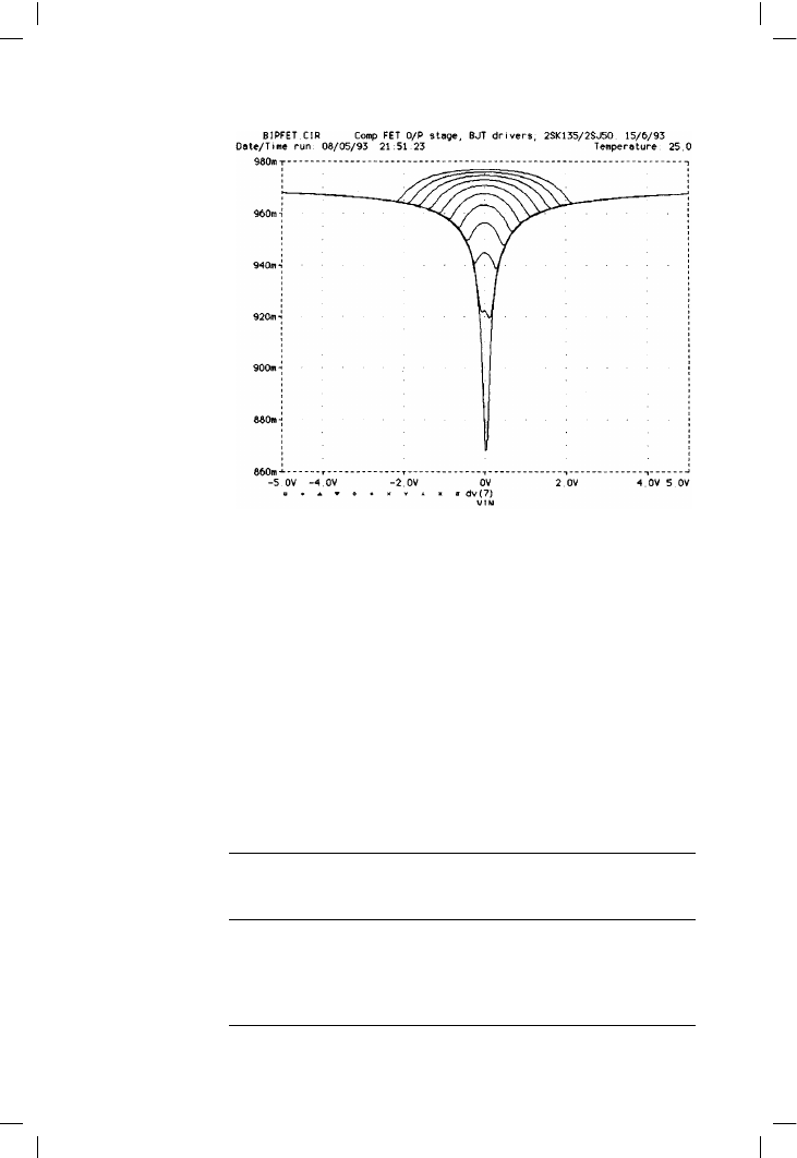
however, as shown, it is rather inefficient in voltage-swing. The crossover
region in Figure 11.5 still has some unpleasant sharp corners, but the total
crossover gain deviation (0.96–0.97 at 8 !) is much smaller than for the
quasi-hybrid (0.78–0.90) and so less high-order harmonic energy is
generated.
Table 11.1 summarises the SPICE curves for 4 and 8 ! loadings. Each was
subjected to Fourier analysis to calculate THD% results for a +/–40 V input.
The BJT results from Chapter 5 are included for comparison.
320
Figure 11.5
Complementary BJT-
FET crossover region
+/–15 V range
Table 11.1
Emitter
Follower
CFP
Quasi
Simple
Quasi
Bax
Triple
Type 1
Simple
MOSFET
Quasi
MOSFET
Hybrid
MOSFET
8 !
0.031% 0.014% 0.069% 0.050% 0.13%
0.47%
0.44%
0.052%
Gain: 0.97
0.97
0.97
0.96
0.97
0.83
0.84
0.97
4 !
0.042% 0.030% 0.079% 0.083% 0.60%
0.84%
0.072% 0.072%
Gain: 0.94
0.94
0.94
0.94
0.92
0.72
0.73
0.94

FET output stages
Power FETs and bipolars: the linearity comparison
There has been much debate as to whether power FETs or bipolar junction
transistors (BJTs) are superior in power amplifier output stages, e.g.
Hawtin
[4]
. As the debate rages, or at any rate flickers, it has often been flatly
stated that power FETs are more linear than BJTs, usually in tones that
suggest that only the truly benighted are unaware of this.
In audio electronics it is a good rule of thumb that if an apparent fact is
repeated times without number, but also without any supporting data, it
needs to be looked at very carefully indeed. I therefore present my own
view of the situation here.
I suggest that it is now well-established that power FETs when used in
conventional Class-B output stages are a good deal less linear than BJTs. The
gain-deviations around the crossover region are far more severe for FETs than
the relatively modest wobbles of correctly biased BJTs, and the shape of the
FET gain-plot is inherently jagged, due to the way in which two square-law
devices overlap. The incremental gain range of a simple FET output stage
is 0.84–0.79 (range 0.05) and this is actually much greater than for the
Bipolar stages examined in Chapter 5; the EF stage gives 0.965–0.972 into
8 ! (range 0.007) and the CFP gives 0.967–0.970 (range 0.003). The smaller
ranges of gain-variation are reflected in the much lower THD figures when
PSpice data is subjected to Fourier analysis.
However, the most important difference may be that the bipolar gain
variations are gentle wobbles, while all FET plots seem to have abrupt
changes that are much harder to linearise with NFB that must decline with
rising frequency. The basically exponential Ic/Vbe characteristics of two
BJTs approach much more closely the ideal of conjugate (i.e. always adding
up to 1) mathematical functions, and this is the root cause of the much
lower crossover distortion.
A close-up examination of the way in which the two types of device begin
conducting as their input voltages increase shows that FETs move abruptly
into the square-law part of their characteristic, while the exponential
behaviour of bipolars actually gives a much slower and smoother start to
conduction.
Similarly, recent work
[5]
shows that less conventional approaches, such as
the CC-CE configuration of Mr Bengt Olsson
[6]
, also suffer from the non-
conjugate nature of FETs, and show sharp changes in gain. Gevel
[7]
shows
that this holds for both versions of the stage proposed by Olsson, using both
N- and P-channel drivers. There are always sharp gain-changes.
FETs in Class-A stages
It occurred to me that the idea that FETs are more linear was based not on
Class-B power-amplifier applications, but on the behaviour of a single
321

Audio Power Amplifier Design Handbook
device in Class-A. It might be argued that the roughly square-law nature of
a FET’s Id/Vgs law is intuitively more linear than the exponential Ic/Vbe law
of a BJT, but it is a bit difficult to know quite how to define linear in this
context. Certainly a square-law device will generate predominantly low-
order harmonics, but this says nothing about the relative amounts
produced.
In truth the BJT/FET contest is a comparison between apples and aardvarks,
the main problem being that the raw transconductance (gm) of a BJT is far
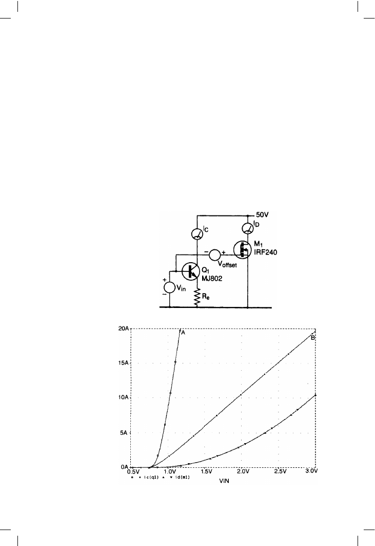
higher than for any power FET. Figure 11.6 illustrates the conceptual test
circuit; both a TO3 BJT (MJ802) and a power-FET (IRF240) have an
increasing DC voltage Vin applied to their base/gate, and the resulting
collector and drain currents from PSpice simulation are plotted in Figure
11.7. Voffset is used to increase the voltage applied to FET M1 by 3.0 V
because nothing much happens below Vgs = 4 V, and it is helpful to have
322
Figure 11.6
The linearity test circuit.
Voffset adds 3 V to the
DC level applied to the
FET gate, purely to
keep the current curves
helpfully adjacent on a
graph
Figure 11.7
Graph of Ic and Id for
the BJT and the FET.
Curve A shows Ic for
the BJT alone, while
Curve B shows the
result for Re = 0.1 !.
The curved line is the
Id result for a power
FET without any
degeneration

FET output stages
the curves on roughly the same axis. Curve A, for the BJT, goes almost
vertically skywards, as a result of its far higher gm. To make the comparison
meaningful, a small amount of local negative feedback is added to Q1 by
Re, and as this emitter degeneration is increased from 0.01 ! to 0.1 !, the
Ic curves become closer in slope to the Id curve.
Because of the curved nature of the FET Id plot, it is not possible to pick an
Re value that allows very close gm equivalence; Re = 0.1 ! was chosen as
a reasonable approximation; see Curve B. However, the important point is
that I think no-one could argue that the FET Id characteristic is more linear
than Curve B.
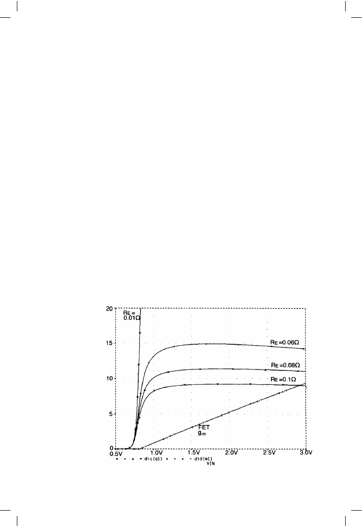
This is made clearer by Figure 11.8, which directly plots transconductance
against input voltage. There is no question that FET transconductance
increases in a beautifully linear manner – but this ‘linearity’ is what results
in a square-law Id increase. The near-constant gm lines for the BJT are a
much more promising basis for the design of a linear amplifier.
To forestall any objections that this comparison is all nonsense because a
BJT is a current-operated device, I add here a small reminder that this is
untrue. The BJT is a voltage operated device, and the base current that
flows is merely an inconvenient side-effect of the collector current induced
by said base voltage. This is why beta varies more than most BJT
parameters; the base current is an unavoidable error rather than the basis of
transistor operation.
The PSpice simulation shown here was checked against manufacturers’
curves for the devices, and the agreement was very good – almost
323
Figure 11.8
Graph of
transconductance
versus input voltage for
BJT and FET. The near-
horizontal lines are
BJT gm for various Re
values

Audio Power Amplifier Design Handbook
unnervingly so. It therefore seems reasonable to rely on simulator output for
these kind of studies – it is certainly infinitely quicker than doing the real
measurements, and the comprehensive power FET component libraries that
are part of PSpice allow the testing to be generalised over a huge number
of component types without actually buying them.
To conclude, I think it is probably irrelevant to simply compare a naked BJT
with a naked FET. Perhaps the vital point is that a bipolar device has much
more raw transconductance gain to begin with, and this can be handily
converted into better linearity by local feedback, i.e. adding a little emitter
degeneration. If the transconductance is thus brought down roughly to FET
levels, the bipolar has far superior large-signal linearity. I must admit to a
sneaking feeling that if practical power BJTs had come along after FETs, they
would have been seized upon with glee as a major step forward in power
amplification.
References
1. Langdon, S Audio amplifier designs using IGBT’s, MOSFETs, and BJTs
Toshiba Application Note X3504, V. 1 Mar 1991.
2. Self, D Sound MOSFET Design Electronics and Wireless World, Sept
1990, p. 760.
3. Self, D MOSFET Audio Output Letter, Electronics and Wireless World,
May 1989, p. 524 (see also reference 2 above).
4. Hawtin, V Letters, Electronics World Dec 1994, p. 1037.
5. Self, D Two-Stage Amplifiers and the Olsson Output Stage Electronics
World, Sept 1995, p. 762.
6. Olsson, B Better Audio From Non-Complements? Electronics World,
Dec 1994, p. 988.
7. Gevel, M Private communication, Jan 1995.
324