ВУЗ: Казахская Национальная Академия Искусств им. Т. Жургенова
Категория: Учебное пособие
Дисциплина: Не указана
Добавлен: 03.02.2019
Просмотров: 17377
Скачиваний: 18

Thermal compensation and thermal dynamics
seem to work directly against quiescent stability, and why these compound
devices are ever used in audio amplifiers remains a mystery to me.)
The drawback with most EF thermal compensation schemes is the slow
response of the heatsink mass to thermal transients, and the obvious
solution is to find some way of getting the sensor closer to one of the output
junctions (symmetry of dissipation is assumed). If TO3 devices are used,
then the flange on which the actual transistor is mounted is as close as we
can get without a hacksaw. This is however clamped to the heatsink, and
almost inaccessible, though it might be possible to hold a sensor under one
of the mounting bolts. A simpler solution is to mount the sensor on the top
of the TO3 can. This is probably not as accurate an estimate of junction
temperature as the flange would give, but measurement shows the top gets
much hotter much faster than the heatsink mass, so while it may appear
unconventional, it is probably the best sensor position for an EF output
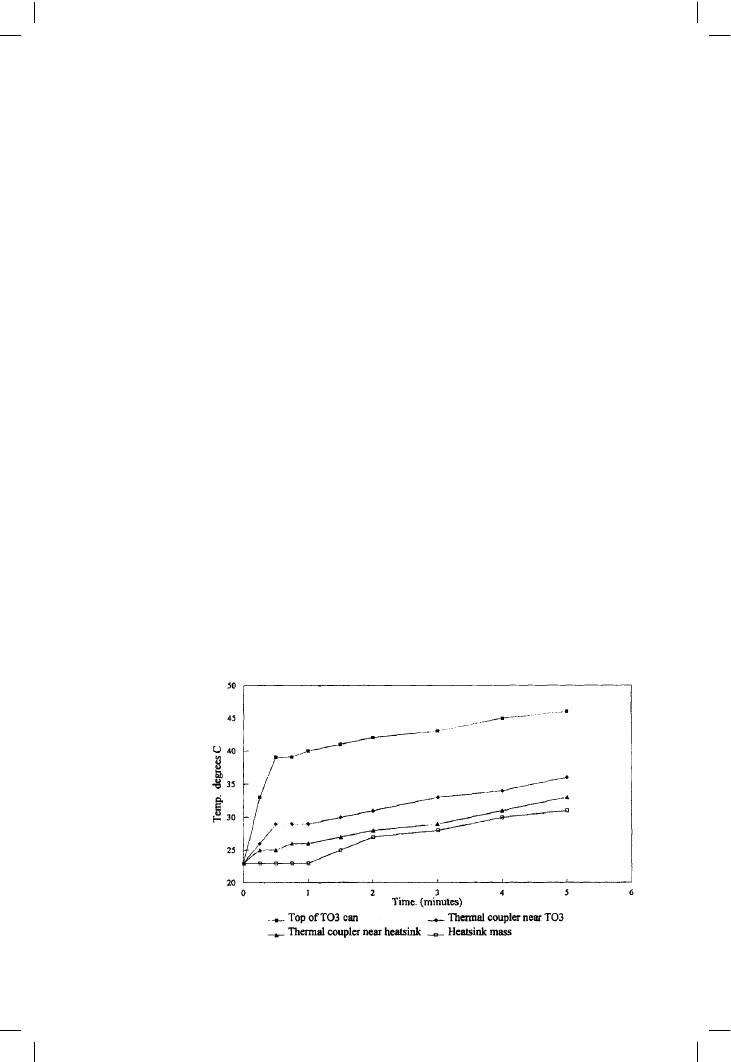
stage. Figure 12.4 shows the results of an experiment designed to test this.
A TO3 device was mounted on a thick aluminium L-section thermal
coupler in turn clamped to a heatsink; this construction is representative of
many designs. Dissipation equivalent to 100 W/8 ! was suddenly initiated,
and the temperature of the various parts monitored with thermocouples.
The graph clearly shows that the top of the TO3 responds much faster, and
with a larger temperature change, though after the first two minutes the
temperatures are all increasing at the same rate. The whole assembly took
more than an hour to asymptote to thermal equilibrium.
Figure 12.5 shows a TO3 output device mounted on a thermal coupling
bar, with a silicone thermal washer giving electrical isolation. The coupler
is linked to the heatsink proper via a second conformal material; this need
not be electrically insulating so highly efficient materials like graphite foil
can be used. This is representative of many amplifier designs, though a
335
Figure 12.4
Thermal response of a
TO3 device on a
large heatsink when
power is suddenly
applied. The top of
the TO3 can responds
most rapidly

Audio Power Amplifier Design Handbook
good number have the power devices mounted directly on the heatsink; the
results hardly differ. A simple thermal-analogue model of Figure 12.5 is
shown in Figure 12.6; the situation is radically simplified by treating each
mass in the system as being at a uniform temperature, i.e. isothermal, and
therefore representable by one capacity each. The boundaries between
parts of the system are modelled, but the thermal capacity of each mass is
concentrated at a notional point. In assuming this we give capacity
elements zero thermal resistance; e.g. both sides of the thermal coupler will
always be at the same temperature. Similarly, elements such as the thermal
washer are assumed to have zero heat capacity, because they are very thin
and have negligible mass compared with other elements in the system.
Thus the parts of the thermal system can be conveniently divided into two
categories; pure thermal resistances and pure thermal capacities. Often this
gives adequate results; if not, more sub-division will be needed. Heat losses
from parts other than the heatsink are neglected.
Real output stages have at least two power transistors; the simplifying
assumption is made that power dissipation will be symmetrical over
anything but the extreme short-term, and so one device can be studied by
slicing the output stage, heatsink, etc. in half.
It is convenient to read off the results directly in °C, rather than temperature
rise above ambient, so Figure 12.6 represents ambient temperature with a
voltage source Vamb that offsets the baseline (node 10) 25°C from
simulator ground, which is inherently at 0°C (0V).
Values of the notional components in Figure 12.6 have to be filled in with
a mixture of calculation and manufacturer’s data. The thermal resistance R1
from junction to case comes straight from the data book, as does the
resistance R2 of the TO3 thermal washer; also R4, the convection
coefficient of the heatsink itself, otherwise known as its thermal resistance
336
Figure 12.5
A TO3 power
transistor attached to a
heatsink by a thermal
coupler. Thermal sensor
is shown on can top;
more usual position
would be on thermal
coupler

Thermal compensation and thermal dynamics
to ambient. This is always assumed to be constant with temperature, which
it very nearly is. Here R4 is 1°C/W, so this is doubled to 2 as we cut the
stage in half to exploit symmetry.
R3 is the thermal resistance of the graphite foil; this is cut to size from a
sheet and the only data is the bulk thermal resistance of 3.85 W/mK, so R3
must be calculated. Thickness is 0.2 mm, and the rectangle area in this
example was 38
× 65 mm. We must be careful to convert all lengths to
metres;
Heat flow/°C =
3.85
× Area
Thickness
=
3.83
× (.038 × .065)
.0002
= 47.3 W/°C
Equation 12.1
So thermal resistance =
1
47.3
= 0.021°C/W
Thermal resistance is the reciprocal of heat flow per degree, so R3 is
0.021°C/W, which just goes to show how efficient thermal washers can be
if they do not have to be electrical insulators as well.
In general all the thermal capacities will have to be calculated, sometimes
from rather inadequate data, thus:
Thermal capacity = Density
× Volume × Specific heat
A power transistor has its own internal structure, and its own internal
thermal model (Figure 12.7). This represents the silicon die itself, the solder
that fixes it to the copper header, and part of the steel flange the header is
welded to. I am indebted to Motorola for the parameters, from an MJ15023
TO3 device
[5]
. The time-constants are all extremely short compared with
heatsinks, and it is unnecessary to simulate in such detail here.
337
Figure 12.6
A thermal/electrical
model of Figure 12.5,
for half of one channel
only. Node 1 is
junction temperature,
node 2 flange
temperature, and so
on. Vamb sets the
baseline to 25°C.
Arrows show heat flow

Audio Power Amplifier Design Handbook
The thermal model of the TO3 junction is therefore reduced to lumped
component C1, estimated at 0.1J/°C; with a heat input of 1 W and no losses
its temperature would increase linearly by 10°C/second. The capacity C2
for the transistor package was calculated from the volume of the TO3 flange
(representing most of the mass) using the specific heat of mild steel. The
thermal coupler is known to be aluminium alloy (not pure aluminium,
which is too soft to be useful) and the calculated capacity of 70J/°C should
be reliable. A similar calculation gives 250 J/°C for the larger mass of the
aluminium heatsink. Our simplifying assumptions are rather sweeping
here, because we are dealing with a substantial chunk of finned metal
which will never be truly isothermal.
338
Figure 12.7
Internal thermal model
for a TO3 transistor. All
the heat is liberated in
the junction structure,
shown as N multiples
of C1 to represent a
typical interdigitated
power transistor
structure
The derived parameters for both output TO3’s and TO-225 AA drivers are
summarised in Table 12.3. The drivers are assumed to be mounted onto
small individual heatsinks with an isolating thermal washer; the data is for
the popular Redpoint SW38-1 vertical heatsink.
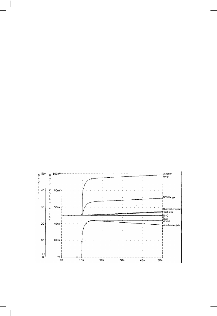
Figures 12.8 and 12.9 show the result of a step-function in heat generation
Table 12.3
Output device
Driver
C1
Junction capacity
J/°C
0.1
0.05
R1
Junction-case resistance
°C/W
0.7
6.25
C2
Transistor package capacity
3.0
0.077
R2
Thermal washer res
0.4
6.9
C3
Coupler capacity
70
–
R3
Coupler-heatsink res
0.021
–
C4
Heatsink capacity
250
20.6
R4
Heatsink convective res
2.0
10.0

Thermal compensation and thermal dynamics
in the output transistor; 20 W dissipation is initiated, corresponding
approximately to a sudden demand for full sinewave power from a
quiescent 100 W amplifier. The junction temperature V(1) takes off near-
vertically, due to its small mass and the substantial thermal resistance
between it and the TO3 flange; the flange temperature V(2) shows a similar
but smaller step as R2 is also significant. In contrast the thermal coupler,
which is so efficiently bonded to the heatsink by graphite foil that they
might almost be one piece of metal, begins a slow exponential rise that will
take a very long time to asymptote. Since after the effect of C1 and C2 have
died away the junction temp is offset by a constant amount from the temp
of C3 and C4, V(1) also shows a slow rise. Note the X-axis of Figure 12.9
must be in kilo-seconds, because of the relatively enormous thermal
capacity of the heatsink.
This shows that a temperature sensor mounted on the main heatsink can
never give accurate bias compensation for junction temperature, even if it
is assumed to be isothermal with the heatsink; in practice there will be
some sensor cooling which will make the sensor temperature slightly
under-read the heatsink temperature V(4). Initially the temperature error
V(1)–V(4) increases rapidly as the TO3 junction heats, reaching 13 degrees
in about 200 ms. The error then increases much more slowly, taking 6
seconds to reach the effective final value of 22 degrees. If we ignore the
thermal-gain effect mentioned above, the long-term Vq error is +44 mV,
i.e. Vq is too high. When this is doubled to allow for both halves of the
339
Figure 12.8
Results for Figure 12.6, with step heat input of 20 W to junction initiated at Time = 10 seconds. Upper plot
shows temperatures, lower the Vbias error for half of output stage