ВУЗ: Казахская Национальная Академия Искусств им. Т. Жургенова
Категория: Учебное пособие
Дисциплина: Не указана
Добавлен: 03.02.2019
Просмотров: 17375
Скачиваний: 18

Audio Power Amplifier Design Handbook
output stage we get +88 mV, which uses up nearly all of the +/–100 mV
error band, without any other inaccuracies. (Hereafter all Vbias/Vq error
figures quoted have been doubled and so apply to a complete output
stage.) Including the thermal gain actually makes little difference over a
10-second timescale; the lower Vq-error trace in Figure 12.8 slowly decays
as the main heatsink warms up, but the effect is too slow to be useful.
The amplifier Vq and Iq will therefore rise under power, as the hot output
device Vbe voltages fall, but the cooler bias generator on the main heatsink
reduces its voltage by an insufficient amount to compensate.
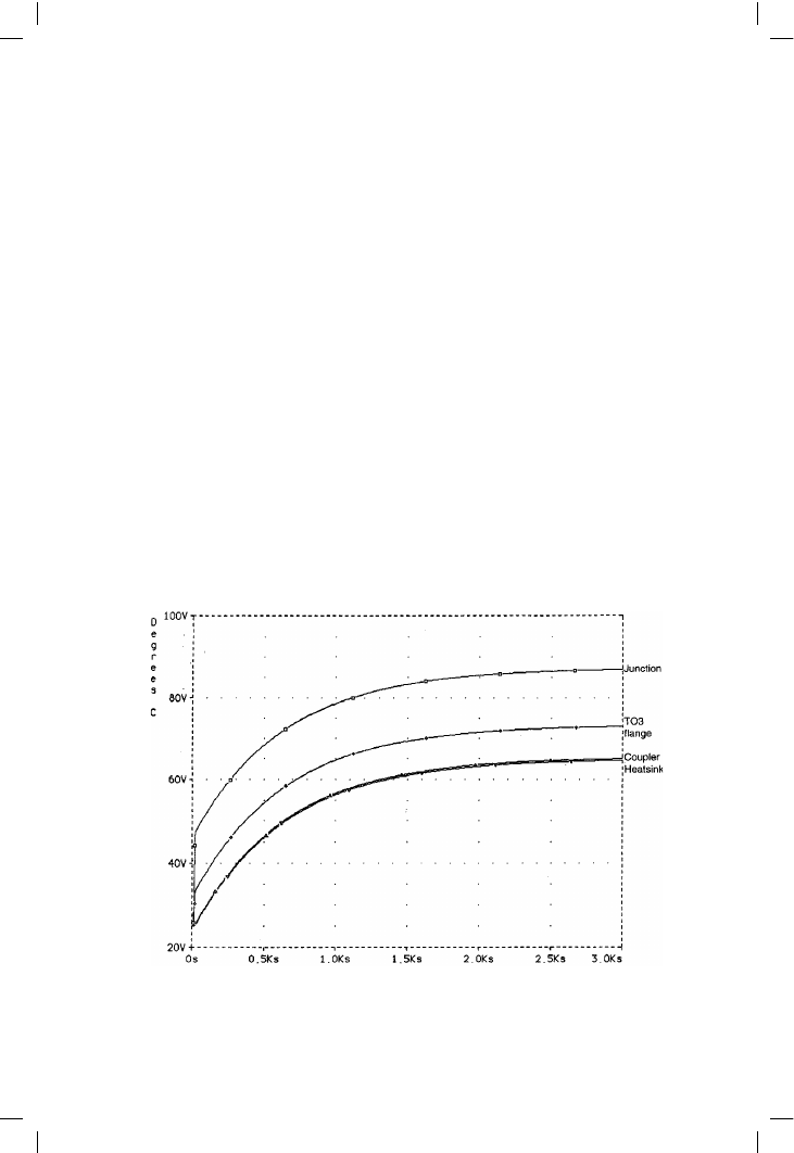
Figure 12.9 shows the long-term response of the system. At least 2500
seconds pass before the heatsink is within a degree of final temperature.
In the past I have recommended that EF output stages should have the
thermal sensor mounted on the top of the TO3 can, despite the mechanical
difficulties. This is not easy to simulate as no data is available for the
thermal resistance between junction and can top. There must be an
additional thermal path from junction to can, as the top very definitely gets
hotter than the flange measured at the very base of the can. In view of the
relatively low temperatures, this path is probably due to internal
convection rather than radiation.
A similar situation arises with TO3P packages (a large plastic package,
twice the size of TO220) for the top plastic surface can get at least 20
degrees hotter than the heatsink just under the device.
340
Figure 12.9
The long-term version of Figure 12.8, showing that it takes over 40 minutes for the heatsink to get within 1
degree of final temperature

Thermal compensation and thermal dynamics
Using the real thermocouple data from page 335, I have estimated the
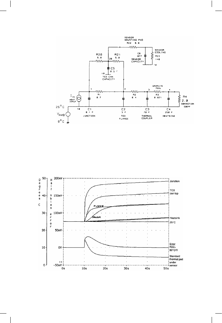
parameters of the thermal paths to the TO3 top. This gives Figure 12.10,
where the values of elements R20, R21, C5 should be treated with
considerable caution, though the temperature results in Figure 12.11 match
reality fairly well; the can top (V20) gets hotter faster than any other
accessible point. R20 simulates the heating path from the junction to the TO3
can and R21 the can-to-flange cooling path, C5 being can thermal capacity.
341
Figure 12.10
Model of EF output
stage with thermal
paths to TO3 can top
modelled by R20,
R21. C5 simulates can
capacity. R23 models
sensor convection
cooling; node 21 is
sensor temperature
Figure 12.11
The simulation results for Figure 12.10; lower plot shows Vbias errors for normal thermal pad under sensor,
and 80°C/W semi-insulator. The latter has near-zero long-term error

Audio Power Amplifier Design Handbook
Figure 12.10 includes approximate representation of the cooling of the
sensor transistor, which now matters. R22 is the thermal pad between
the TO3 top and the sensor, C6 the sensor thermal capacity, and R23 is the
convective cooling of the sensor, its value being taken as twice the
datasheet free-air thermal resistance as only one face is exposed.
Putting the sensor on top of the TO3 would be expected to reduce the
steady-state bias error dramatically. In fact, it overdoes it, as after factoring
in the thermal-gain of a Vbe-multiplier in an EF stage, the bottom-most
trace of Figure 12.11 shows that the bias is over-compensated; after the
initial positive transient error, Vbias falls too low giving an error of –30 mV,
slowly worsening as the main heatsink warms up. If thermal-gain had been
ignored, the simulated error would have apparently fallen from +44 (Figure
12.8) to +27 mV; apparently a useful improvement, but actually illusory.
Since the new sensor position over-compensates for thermal errors, there
should be an intermediate arrangement giving near-zero long-term error. I
found this condition occurs if R22 is increased to 80°C/W, requiring some
sort of semi-insulating material rather than a thermal pad, and gives the
upper error trace in the lower half of Figure 12.11. This peaks at +30 mV
after 2 seconds, and then decays to nothing over the next twenty. This is
much superior to the persistent error in Figure 12.8, so I suggest this new
technique may be useful.
Modelling the CFP output stage
In the CFP configuration, the output devices are inside a local feedback
loop, and play no significant part in setting Vq, which is dominated by
thermal changes in the driver Vbe’s. Such stages are virtually immune to
thermal runaway; I have found that assaulting the output devices with a
powerful heat gun induces only very small Iq changes. Thermal compensa-
tion is mechanically simpler as the Vbe-multiplier transistor is usually
mounted on one of the driver heatsinks, where it aspires to mimic the driver
junction temperature.
It is now practical to make the bias transistor of the same type as the drivers,
which should give the best matching of Vbe
[6]
, though how important this
is in practice is uncertain. This also avoids the difficulty of trying to attach
a small-signal (probably TO92) transistor package to a heatsink.
Since it is the driver junctions that count, output device temperatures are
here neglected. The thermal parameters for a TO225AA driver (e.g.
MJE340/350) on the SW38-1 vertical heatsink are shown in Table 12.3; the
drivers are on individual heatsinks so their thermal resistance is used
directly, without doubling.
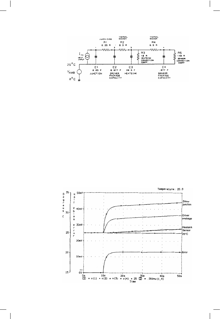
In the simulation circuit (Figure 12.12) V(3) is the heatsink temperature; the
sensor transistor (also MJE340) is mounted on this sink with thermal washer
342

Thermal compensation and thermal dynamics
R4, and has thermal capacity C4. R5 is convective cooling of the sensor. In
this case the resulting differences in Figure 12.13 between sink V(3) and
sensor V(4) are very small.
We might expect the CFP delay errors to be much shorter than in the EF;
however, simulation with a heat step-input suitably scaled down to 0.5 W
(Figure 12.13) shows changes in temperature error V(1)–V(4) that appear
rather paradoxical; the error reaches 5 degrees in 1.8 seconds, levelling out
at 6.5 degrees after about 6 seconds. This is markedly slower than the EF
case, and gives a total bias error of +13 mV, which after doubling to +26 mV
is well outside the CFP error band of +/–10 mV.
The initial transients are slowed down by the much smaller step heat
input, which takes longer to warm things up. The final temperature
however, is reached in 500 rather than 3000 seconds, and the timescale
is now in hundreds rather than thousands of seconds. The heat input is
343
Figure 12.12
Model of a CFP stage.
Driver transistor is
mounted on a small
heatsink, with sensor
transistor on the other
side. Sensor dynamics
and cooling are
modelled by R4, C4
and R5
Figure 12.13
Simulation results for
CFP stage, with step
heat input of 0.5 W.
Heatsink and sensor
are virtually
isothermal, but there
is a persistent error
as driver is always
hotter than heatsink
due to R1, R2

Audio Power Amplifier Design Handbook
smaller, but the driver heatsink capacity is also smaller, and the overall
time-constant is less.
It is notable that both timescales are much longer than musical
dynamics.
The integrated absolute error criterion
Since the thermal sensor is more or less remote from the junction whose
gyrations in temperature will hopefully be cancelled out, heat losses and
thermal resistances cause the temperature change reaching the sensor to be
generally too little and too late for complete compensation.
As in the previous section, all the voltages and errors here are for one-half
of an output stage, using symmetry to reduce the work involved. These
half-amplifiers are used throughout this chapter, for consistency, and the
error voltages are only doubled to represent reality (a complete output
stage) when they are compared against the tolerance bands previously
quoted.
We are faced with errors that vary not only in magnitude, but also in their
persistence over time; judgement is required as to whether a prolonged
small error is better than a large error which quickly fades away.
The same issue faces most servomechanisms, and I borrow from Control
Theory the concept of an Error Criterion which combines magnitude and
time into one number
[7],[8]
. The most popular criterion is the Integrated
Absolute Error (IAE) which is computed by integrating the absolute-value of
the error over a specified period after giving the system a suitably
provocative stimulus; the absolute-value prevents positive and negative
errors cancelling over time. Another common criterion is the Integrated
Square Error (ISE) which solves the polarity problem by squaring the error
before integration – this also penalises large errors much more than small
ones. It is not immediately obvious which of these is most applicable to
bias-control and the psychoacoustics of crossover distortion that changes
with time, so I have chosen the popular IAE.
One difficulty is that the IAE error criterion for bias voltage tends to
accumulate over time, due to the integration process, so any constant bias
error quickly comes to dominate the IAE result. In this case, the IAE is little
more than a counter-intuitive way of stating the constant error, and must be
quoted over a specified integration time to mean anything at all. This is why
the IAE concept was not introduced earlier in this chapter.
Much more useful results are obtained when the IAE is applied to a
situation where the error decays to a very small value after the initial
transient, and stays there. This can sometimes be arranged in amplifiers, as
I hope to show. In an ideal system where the error decayed to zero without
overshoot, the IAE would asymptote to a constant value after the initial
344