ВУЗ: Казахская Национальная Академия Искусств им. Т. Жургенова
Категория: Учебное пособие
Дисциплина: Не указана
Добавлен: 03.02.2019
Просмотров: 17373
Скачиваний: 18

Thermal compensation and thermal dynamics
transient. In real life, residual errors make the IAE vary slightly with time, so
for consistency all the IAE values given here are for 30 seconds after the
step-input.
Improved thermal compensation: the emitter-follower stage
It was shown above that the basic emitter-follower (EF) stage with the
sensor on the main heatsink has significant thermal attenuation error and
therefore under-compensates temperature changes. (The Vq error is
+44 mV, the positive sign showing it is too high. If the sensor is on the TO3
can top it over-compensates instead) (Vq error –30 mV).
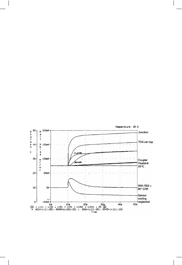
If an intermediate configuration is contrived by putting a layer of controlled
thermal resistance (80°C/W) between the TO3 top and the sensor, then the
50-second timescale component of the error can be reduced to near-zero.
This is the top error trace in bottom half of Figure 12.14; the lower trace
shows the wholly misleading result if sensor heat losses are neglected in
this configuration.
Despite this medium-term accuracy, if the heat input stimulus remains
constant over the very long-term (several kilo-seconds) there still remains a
345
Figure 12.14
EF behaviour with semi-insulating pad under sensor on TO3 can top. The sensor in the upper temperature plot
rises more slowly than the flange, but much faster than the main heatsink or coupler. In lower Vq-error section,
upper trace is for a 80°C/W thermal resistance under the sensor, giving near-zero error. Bottom trace shows
serious effect of ignoring sensor-cooling in TO3-top version

Audio Power Amplifier Design Handbook
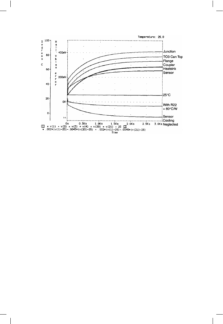
very slow drift towards over-compensation due to the slow heating of the
main heatsink (Figure 12.15).
This long-term drift is a result of the large thermal inertia of the main
heatsink and since it takes 1500 seconds (25 minutes) to go from zero to
–32 mV is of doubtful relevance to the time-scales of music and signal level
changes. On doubling to –64 mV, it remains within the EF Vq tolerance of
+/–100 mV. On the shorter 50-second timescale, the half-amplifier error
remains within a +/–1 mV window from 5 seconds to 60 seconds after the
step-input.
For the EF stage, a very-long-term drift component will always exist so long
as the output device junction temperature is kept down by means of a main
heatsink that is essentially a weighty chunk of finned metal.
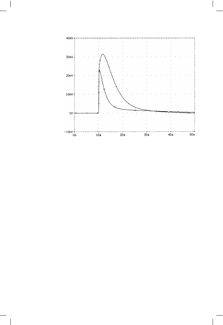
The EF system stimulus is a 20 W step as before, being roughly worst-case
for a 100 W amplifier. Using the 80°C/W thermal semi-insulator described
above gives the upper error trace in Figure 12.16, and an IAE of 254 mV-sec
after 30 seconds. This is relatively large because of the extra time-delay
caused by the combination of an increased R22 with the unchanged sensor
thermal capacity C6. Once more, this figure is for a half-amplifier, as are all
IAEs in this chapter.
346
Figure 12.15
Over a long timescale, the lower plot shows that the Vq error, although almost zero in Figure 12.14, slowly
drifts into over-compensation as the heatsink temperature (upper plot) reaches asymptote

Thermal compensation and thermal dynamics
Up to now I have assumed that the temperature coefficient of a Vbe-
multiplier bias generator is rigidly fixed at –2 mV/°C times the Vbe-
multiplication factor, which is about 4.5
× for EF and 2× for CFP. The
reason for the extra thermal gain displayed by the EF was set out on
page 334.
The above figures are for both halves of the output stage, so the half-
amplifier value for EF is –4.5 mV/°C, and for CFP –2 mV/°C. However . . .
if we boldly assume that the Vbias generator can have its thermal
coefficient varied at will, the insulator and its aggravated time-lag can be
eliminated. If a thermal pad of standard material is once more used
between the sensor and the TO3 top, the optimal Vbias coefficient for
minimum error over the first 40 seconds proves to be –2.8 mV/°C, which is
usefully less than –4.5. The resulting 30-second IAE is 102 mV-sec, more
than a two times improvement; see the lower trace in Figure 12.16, for
comparison with the semi-insulator method described above.
In view of the fixed time-constants, dependant upon a certain weight of
metal being required for heat dissipation, it appears that the only way this
performance could be significantly improved upon might be to introduce a
new kind of output transistor with an integral diode that would sense the
actual junction temperature, being built into the main transistor junction
structure. Although it would be of immense help to amplifier makers, no-
one seems to be keen to do this.
From here on I am going to assume that a variable-temperature-coefficient
(tempco) bias generator can be made when required; the details of how to
347
Figure 12.16
The transient error for
the semi-insulating pad
and the low-tempco
version. The latter
responds much faster,
with a lower peak
error, and gives less
than half the Integrated
Absolute Error (IAE)

Audio Power Amplifier Design Handbook
do it are not given here. It is an extremely useful device, as thermal
attenuation can then be countered by increasing the thermal gain; it does
not however help with the problem of thermal delay.
In the second EF example above, the desired tempco is –2.8 mV/°C, while
an EF output stage plus Vbe-multiplier has an actual tempco of –4.5 mV/°C.
(This inherent thermal gain in the EF was explained on page 334.) In this
case we need a bias generator that has a smaller tempco than the standard
circuit. The conventional EF with its temp sensor on the relatively cool
main heatsink would require a larger tempco than standard.
A potential complication is that amplifiers should also be reasonably
immune to changes in ambient temperature, quite apart from changes due
to dissipation in the power devices. The standard tempco gives a close
approach to this automatically, as the Vbe-multiplication factor is naturally
almost the same as the number of junctions being biased. However, this
will no longer be true if the tempco is significantly different from standard,
so it is necessary to think about a bias generator that has one tempco for
power-device temperature changes, and another for ambient changes. This
sounds rather daunting, but is actually fairly simple.
Improved compensation for the CFP output stage
As revealed on page 329, the Complementary-Feedback-Pair (CFP) output
stage has a much smaller bias tolerance of +/–10 mV for a whole amplifier,
and surprisingly long time-constants. A standard CFP stage therefore has
larger relative errors than the conventional Emitter-Follower (EF) stage with
thermal sensor on the main heatsink; this is the opposite of conventional
wisdom. Moving the sensor to the top of the TO3 can was shown to
improve the EF performance markedly, so we shall attempt an analogous
improvement with driver compensation.
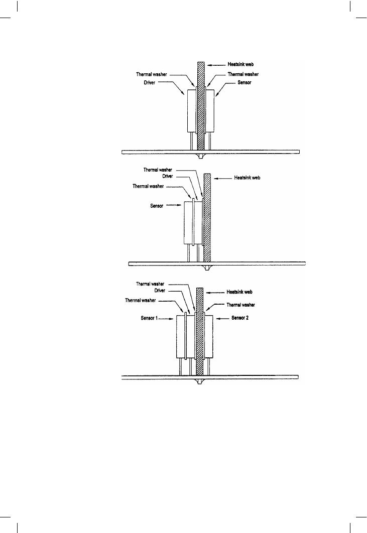
The standard CFP thermal compensation arrangements have the sensor
mounted on the driver heatsink, so that it senses the heatsink temperature
rather than that of the driver itself. (See Figure 12.17a for mechanical
arrangement, and Figure 12.18 for thermal model.) As in the EF, this gives
a constant long-term error due to the sustained temperature difference
between the driver junction and heatsink mass; see the upper traces in
Figure 12.20, plotted for different bias tempcos. The CFP stimulus is a
0.5 W step, as before. This constant error cannot be properly dealt with by
choosing a tempco that gives a bias error passing through a zero in the first
fifty seconds, as was done for the EF case with a TO3-top sensor, as the
heatsink thermal inertia causes it to pass through zero very quickly and
head rapidly South in the direction of ever-increasing negative error. This is
because it has allowed for thermal attenuation but has not decreased
thermal delay. It is therefore pointless to compute an IAE for this
configuration.
348

Thermal compensation and thermal dynamics
A better sensor position
By analogy with the TO3 and TO3P transistor packages examined earlier,
it will be found that driver packages such as TO225AA on a heatsink get
hotter faster on their exposed plastic face than any other accessible point.
It looks as if a faster response will result from putting the sensor on top of
the driver rather than on the other side of the sink as usual. With the
Redpoint SW 38-1 heatsink this is fairly easy as the spring-clips used to
349
Figure 12.17
a The sensor transistor
on the driver
heatsink
b An improved
version, with the
sensor mounted on
top of the driver
itself, is more
accurate
c Using two sensors to
construct a junction-
estimator