ВУЗ: Казахская Национальная Академия Искусств им. Т. Жургенова
Категория: Учебное пособие
Дисциплина: Не указана
Добавлен: 03.02.2019
Просмотров: 17372
Скачиваний: 18

Audio Power Amplifier Design Handbook
secure one plastic package will hold a stack of two TO225AA’s with only
a little physical persuasion. A standard thermal pad is used between the top
of the driver and the metal face of the sensor, giving the sandwich shown
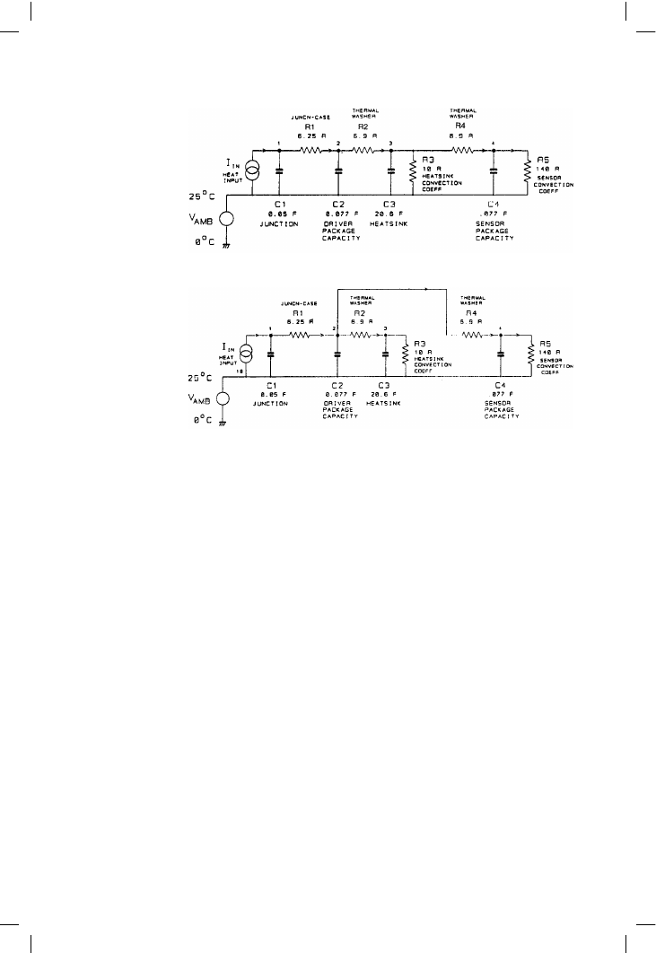
in Figure 12.17b. The thermal model is Figure 12.19. This scheme greatly
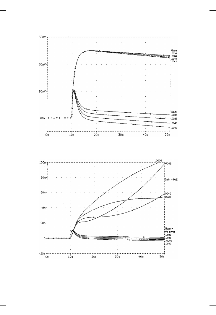
reduces both thermal attenuation and thermal delay (lower traces in Figure
12.20) giving an error that falls within a +/–1 mV window after about 15.5
seconds, when the tempco is set to –3.8 mV/°C. The IAE computes to
52 mV, as shown in Figure 12.21, which demonstrates how the IAE
criterion tends to grow without limit unless the error subsides to zero. This
value is a distinct improvement on the 112 mV IAE which is the best that
could be got from the EF output.
The effective delay is much less because the long heatsink time-constant is
now partly decoupled from the bias compensation system.
A junction-temperature estimator
It appears that we have reached the limit in what can be done, as it is hard
to get one transistor closer to another than they are in Figure 12.17b. It is
however possible to get better performance, not by moving the sensor
position, but by using more of the available information to make a better
estimate of the true driver junction temperature. Such estimator subsystems
are widely used in servo control systems where some vital variable is
inaccessible, or only knowable after such a time-delay as to render the data
useless
[9]
. It is often almost as useful to have a model system, usually just
350
Figure 12.18
Thermal circuit of
normal CFP sensor
mounting on heatsink.
R3 is the convective
cooling of the
heatsink, while R5
models heat losses
from the sensor body
itself
Figure 12.19
Thermal circuit of
driver-back mounting
of sensor. The large
heatsink time-constant
R2–C2 is no longer
in the direct thermal
path to the sensor, so
the compensation is
faster and more
accurate

Thermal compensation and thermal dynamics
Figure 12.20
The Vq errors for normal and improved sensor mounting, with various tempcos. The improved method can
have its tempco adjusted to give near-zero error over this timescale. Not so for the usual method
Figure 12.21
The Vq error and IAE for the improved sensor mounting method on driver back. Error is much smaller, due
both to lower thermal attenuation and less delay. Best IAE is 52 mV-sec (with gain = 0.0038); twice as good
as the best EF version
351

Audio Power Amplifier Design Handbook
an abstract set of gains and time-constants, which all give an estimate of
what the current value of the unknown variable must be, or ought to be.
The situation here is similar, and the first approach makes a better guess at
the junction temperature V(1) by using the known temperature drop
between the package and the heatsink. The inherent assumption is made
that the driver package is isothermal, as it is modelled by one temperature
value V(2).
If two sensors are used, one placed on the heatsink as usual, and the other
on top of the driver package, as described above, (Figure 12.17c), then
things get interesting. Looking at Figure 12.19, it can be seen that the
difference between the driver junction temperature and the heatsink is due
to R1 and R2; the value of R1 is known, but not the heat flow through it.
Neglecting small incidental losses, the temperature drop through R1 is
proportional to the drop through R2. Since C2 is much smaller than C3, this
should remain reasonably true even if there are large thermal transients.
Thus, measuring the difference between V(2) and V(3) allows a reasonable
estimate of the difference between V(1) and V(2); when this difference is
added to the known V(2), we get a rather good estimation of the
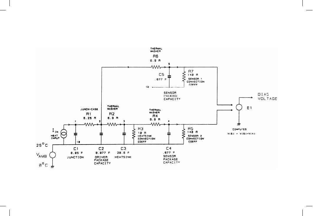
inaccessible V(1). This system is shown conceptually in Figure 12.22,
which gives only the basic method of operation; the details of the real
circuitry must wait until we have decided exactly what we want it to do.
We can only measure V(2) and V(3) by applying thermal sensors to them, as
in Figure 12.17c, so we actually have as data the sensor temperatures V(4)
and V(5). These are converted to bias voltage and subtracted, thus estimating
the temperature drop across R1. The computation is done by Voltage-
Controlled-Voltage-Source E1, which in PSpice can have any equation
assigned to define its behaviour. Such definable VCVSs are very handy as
little analogue computers that do calculations as part of the simulation
model. The result is then multiplied by a scaling factor called estgain which
is incorporated into the defining equation for E1, and is adjusted to give the
minimum error; in other words the variable-tempco bias approach is used to
allow for the difference in resistance between R1 and R2.
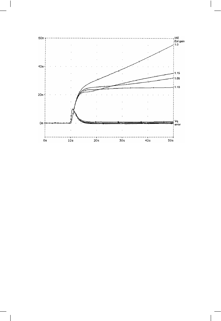
The results are shown in Figure 12.23, where an estgain of 1.10 gives the
minimum IAE of 25 mV-sec. The transient error falls within a +/–1 mV
window after about 5 seconds. This is a major improvement, at what
promises to be little cost.
A junction estimator with dynamics
The remaining problem with the junction-estimator scheme is still its
relatively slow initial response; nothing can happen before heat flows
through R6 into C5, in Figure 12.22. It will take even longer for C4 to
respond, due to the inertia of C3, so we must find a way to speed up the
dynamics of the junction-estimator.
352

Figure 12.22
Conceptual diagram of
the junction-estimator.
Controlled-voltage-
source E1 acts as an
analogue computer
performing the scaling
and subtraction of the
two sensor
temperatures V(4) and
V(5), to derive the bias
voltage

Audio Power Amplifier Design Handbook
The first obvious possibility is the addition of phase-advance to the
forward bias-compensation path. This effectively gives a high gain
initially, to get things moving, which decays back over a carefully-set
time to the original gain value that gave near-zero error over the
50-second timescale. The conceptual circuit in Figure 12.24 shows the
phase-advance circuitry added to the compensation path; the signal is
attenuated 100
× by R50 and R51, and then scaled back up to the same
level by VCVS E2, which is defined to give a gain of 110 times
incorporating estimated gain = 1.10. C causes fast changes to bypass the
attenuation, and its value in conjunction with R50, R51 sets the degree of
phase-advance or lead. The slow behaviour of the circuit is thus
unchanged, but transients pass through C and are greatly amplified by
comparison with steady-state signals.
The result on the initial error transient of varying C around its optimal value
can be seen in the expanded view of Figure 12.25. The initial rise in Vq
error is pulled down to less than a third of its value if C is made 10 µF; with
a lower C value the initial peak is still larger than it need be, while a higher
value introduces some serious undershoot that causes the IAE to rise again,
as seen in the upper traces in Figure 12.26. The big difference between no
phase-advance, and a situation where it is even approximately correct, is
very clear.
354
Figure 12.23
Simulation results for the junction-estimator, for various values of estgain. The optimal IAE is halved to
25 mV-sec; compare with Figure 12.21