ВУЗ: Казахская Национальная Академия Искусств им. Т. Жургенова
Категория: Учебное пособие
Дисциплина: Не указана
Добавлен: 03.02.2019
Просмотров: 17369
Скачиваний: 18

Audio Power Amplifier Design Handbook
a CFP bias circuit has its tempco varied by increasing V1 in 100 mV steps;
in each case the value of R2 is then reduced to bring Vbias back to the
desired value, and the tempco is increased.
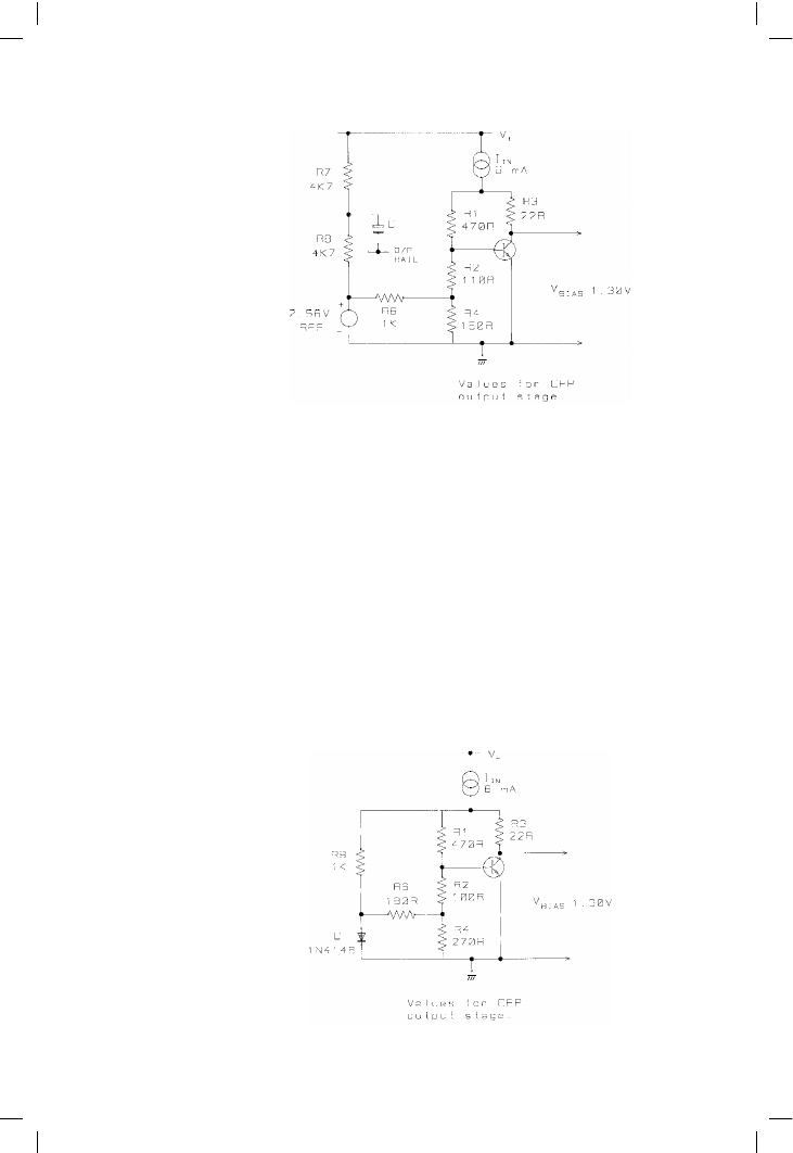
A practical circuit is shown in Figure 12.29, using a 2.56 V bandgap refer-
ence to generate the extra voltage across R4. This reference has to work
outside the bias generator rails, so its power-feed resistors R7, R8 are boot-
strapped by C from the amplifier output, as in the Trimodal amplifier design.
Ambient temperature changes
Power amplifiers must be reasonably immune to ambient temperature
changes, as well as changes due to dissipation in power devices.
The standard compensation system deals with this pretty well, as the
360
Figure 12.29
Shows a practical
version of a Vbe
multiplier with
increased tempco. The
extra voltage source is
derived from the
bandgap reference by
R6, R4. Tempco is
increased to
–5.3 mV/°C
Figure 12.30
Practical Vbe multiplier
with increased tempco,
and also improved
correction for ambient
temperature changes,
by using diode D to
derive the extra voltage

Thermal compensation and thermal dynamics
Vbe-multiplication factor is inherently almost the same as the number of
junctions being biased. This is no longer true if the tempco is significantly
modified. Ideally we require a bias generator that has one increased
tempco for power-device temperature changes only, and another standard
tempco for ambient changes affecting all components. One approach to
this is Figure 12.30, where V1 is derived via R6, R4 from a silicon diode
rather than a bandgap reference, giving a voltage reducing with tem-
perature. The tempco for temperature changes to Q1 only is –4.0 mV/°C,
while the tempco for global temperature changes to both Q1 and D1 is
lower at –3.3 mV/°C. Ambient temperatures vary much less than output
device junction temperatures, which may easily range over 100 °C.
Creating a lower tempco
Earlier in this chapter I showed that an EF output stage has ‘thermal gain’ in
that the thermal changes in Vq make it appear that the tempco of the Vbias
generator is higher than it really is. This is because the bias generator is set
up to compensate for four base-emitter junctions, but in the EF output
configuration the drivers have a roughly constant power dissipation with
changing output power, and therefore do not change much in junction
temperature. The full effect of the higher tempco is thus felt by the output
junctions, and if the sensor is placed on the power device itself rather than
the main heatsink, to reduce thermal delay, then the amplifier can be
seriously over compensated for temperature. In other words, after a burst of
power Vq will become too low rather than too high, and crossover
distortion will appear. We now need a Vbias generator with a lower tempco
than the standard circuit.
The principle is exactly analogous to the method of increasing the tempco.
In Figure 12.31, a voltage source is inserted in the upper leg of potential
361
Figure 12.31
The principle of a
Vbe multiplier with
reduced tempco. The
values shown give
–3.1 mV/°C

Audio Power Amplifier Design Handbook
divider R1, R2; the required Vbe-multiplication factor for the same Vbias is
reduced, and so therefore is the tempco.
Table 12.6 shows how this works as V1 is increased in 100 mV steps. R1
has been varied to keep Vbias constant, in order to demonstrate the
symmetry of resistor values with Table 12.5; in reality R2 would be the
variable element, for the safety reasons described above.
Current compensation
Both bias generators in Figure 12.27 are fitted with a current-compensation
resistor R3. The Vbe multiplier is a very simple shunt regulator, with low
loop gain, and hence shows a significant series resistance. In other words,
the Vbias generated shows unwanted variations in voltage with changes in
the standing current through it. R3 is added to give first-order cancellation
of Vbias variations caused by these current changes. It subtracts a
correction voltage proportional to this current. Rather than complete
cancellation, this gives a peaking of the output voltage at a specified
current, so that current changes around this peak value cause only minor
voltage variations. This peaking philosophy is widely used in IC bias
circuitry.
R3 should never be omitted, as without it mains voltage fluctuations can
seriously affect Vq. Table 12.4 shows that the optimal value for peaking at
6 mA depends strongly on the Vbe multiplication factor.
Figure 6.14 demonstrates the application of this method to the Class-B
amplifier. The graph shows the variation of Vbias with current for different
values of R3. The slope of the uncompensated (R3 = 0) curve at 6 mA is
approx. 20 !, and this linear term is cancelled by setting R3 to 18 ! in
Figure 6.13.
The current through the bias generator will vary because the VAS current
source is not a perfect circuit element. Biasing this current source with the
usual pair of silicon diodes does not make it wholly immune to supply-rail
362
Table 12.6
V1
mV
Vbias
V
R1
!
Tempco
mV/C
0
1.287
470
–3.6
100
1.304
390
–3.3
200
1.287
330
–3.1
300
1.286
260
–2.8
400
1.285
190
–2.5

Thermal compensation and thermal dynamics
variations. I measured a generic amplifier (essentially the original Class-B
Blameless design) and varied the incoming mains from 212 V to 263 V,
a range of 20%. This in these uncertain times is perfectly plausible for a
power amplifier travelling around Europe. The VAS current-source output
varied from 9.38 mA to 10.12 mA, which is a 7.3% range. Thanks to the
current-compensating resistor in the bias generator, the resulting change
in quiescent voltage Vq across the two Re’s is only from 1.1 mV (264 V
mains) to 1.5 mV (212 V mains). This is a very small absolute change of
0.4 mV, and within the Vq tolerance bands. The ratio of change is greater,
because Vbias has had a large fixed quantity (the device Vbe’s) subtracted
from it, so the residue varies much more. Vq variation could be further
suppressed by making the VAS current source more stable against supply
variations.
The finite ability of even the current-compensated bias generator to cope
with changing standing current makes a bootstrapped VAS collector load
much less attractive than the current-source version; from the above data,
it appears that Vq variations will be at least three times greater.
A quite different approach reduces Vbias variations by increasing the
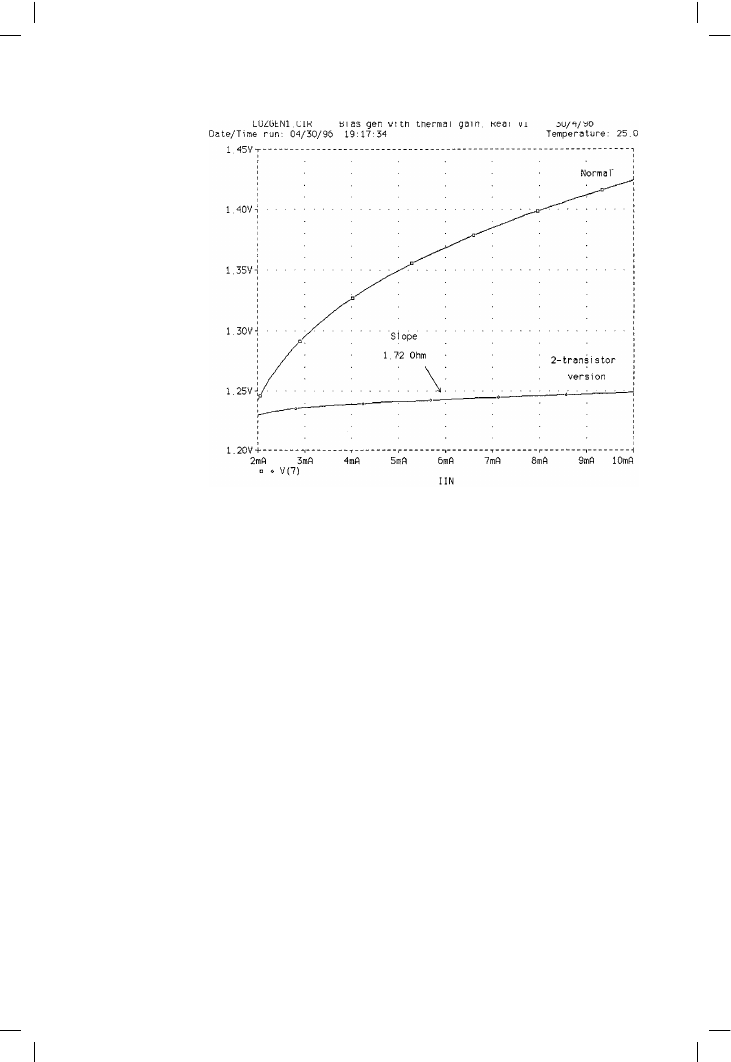
loop gain in the Vbe multiplier. Figure 12.32 shows the circuit of a two-
transistor version that reduces the basic resistance slope from 20 to 1.7 !.
The first transistor is the sensor. An advantage is that Vbias variations will
be smaller for all values of VAS current, and no optimisation of a resistor
value is required. A drawback is slightly greater complexity in an area
where reliability is vital. Figure 12.33 compares the two-transistor
configuration with the standard version (without R3). Multi-transistor
feedback loops raise the possibility of instability and oscillation, and this
must be carefully guarded against, as it is unlikely to improve amplifier
reliability.
363
Figure 12.32
Circuit of a two-
transistor Vbe multiplier.
The increased loop
gain holds Vbias more
constant against current
changes

Audio Power Amplifier Design Handbook
This section of the Thermal Dynamics chapter describes simple Vbias
generators with tempcos ranging from –2.5 to –6.9 mV/°C. It is hoped that
this, in combination with the techniques described earlier, will enable the
design of Class-B amplifiers with greater bias accuracy, and therefore less
afflicted by crossover distortion.
Thermal dynamics in reality
One of the main difficulties in the study of amplifier thermal dynamics is
that some of the crucial quantities, such as transistor junction temperatures,
are not directly measurable. The fact that bias conditions are altering is
usually recognised from changes in the THD residual as viewed on a scope.
However, these temperatures are only a means to an end – low distortion.
What really matters is the crossover distortion produced by the output
stage. Measuring this gets to the heart of the matter. The method is as
follows. The amplifier under study is deliberately underbiased by a modest
amount. I chose a bias setting that gave about 0.02% THD with a peak
responding measurement mode. This is to create crossover spikes that are
clear of the rest of the THD residual, to ensure the analyser is reading these
spikes and ignoring noise and other distortions at a lower level. The AP
System-1 has a mode that plots a quantity against time (it has to be said that
the way to do this is not at all obvious from the AP screen menus –
essentially ‘time’ is treated as an external stimulus – but it is in the manual)
and this effectively gives that most desirable of plots – crossover conditions
364
Figure 12.33
The two-transistor
configuration gives a
consistently lower
series resistance, and
hence Vbias variation
with current,
compared with the
standard version
without R3